
Method of forming semiconductor structure

a technology of semiconductor structure and semiconductor components, applied in the direction of semiconductor/solid-state device manufacturing, basic electric elements, electric apparatus, etc., can solve the problem of reducing the size of features, and achieve the effect of improving device performance, enhancing the dimension of the device, and preferably the structur

Active Publication Date: 2020-06-02
UNITED MICROELECTRONICS CORP +1
View PDF5 Cites 0 Cited by
  • Summary
  • Abstract
  • Description
  • Claims
  • Application Information

AI Technical Summary

Benefits of technology

The present invention provides a method of forming a semiconductor structure using a multiple patterning process. This method allows for the formation of target patterns or structures using a simplified process flow under a maintained pitch. The method utilizes a sidewall image transfer technique to form alternately arranged spacers and mandrels, which are then used as a mask to define the target patterns or structures. This approach allows for the formation of semiconductor structures with uniform, enlarged dimensions in a denser layout, leading to better device performance. Overall, this method provides a more efficient and effective means of forming semiconductor structures.

Problems solved by technology

As feature sizes are decreased by the complexity of currently integrated circuits, the existing single patterning process has met its bottleneck to successfully render the features.
That is, the overlay accuracy and the resolution among this feature have to push the lithographic limit further to create even smaller, more densely packed devices.

Method used


Image

  • Method of forming semiconductor structure
  • Method of forming semiconductor structure
  • Method of forming semiconductor structure

Examples


first embodiment

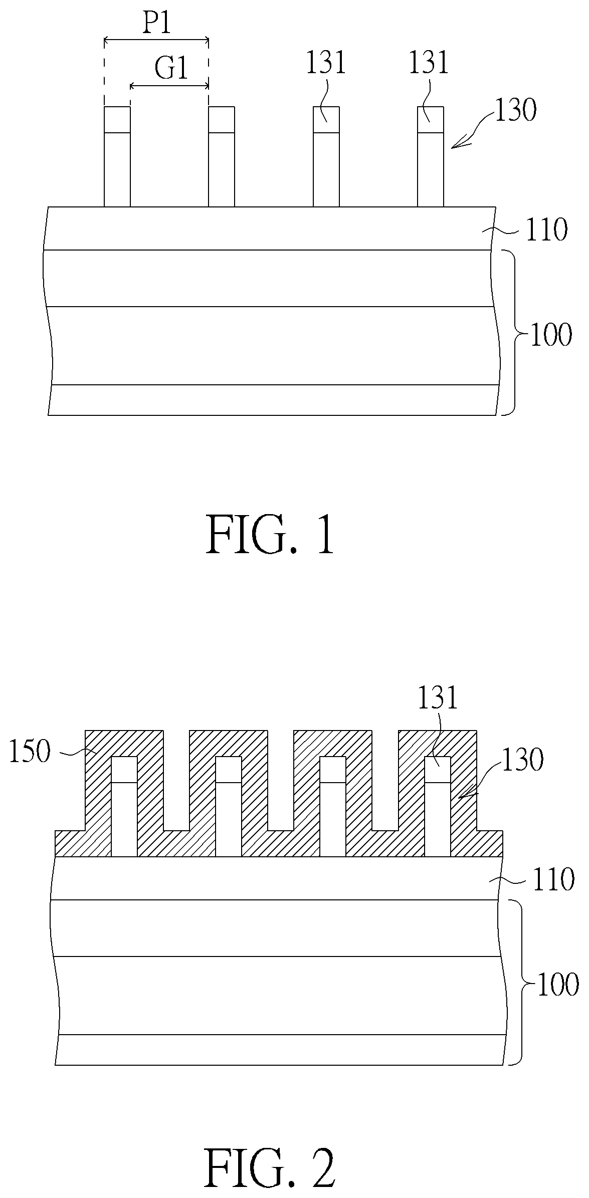
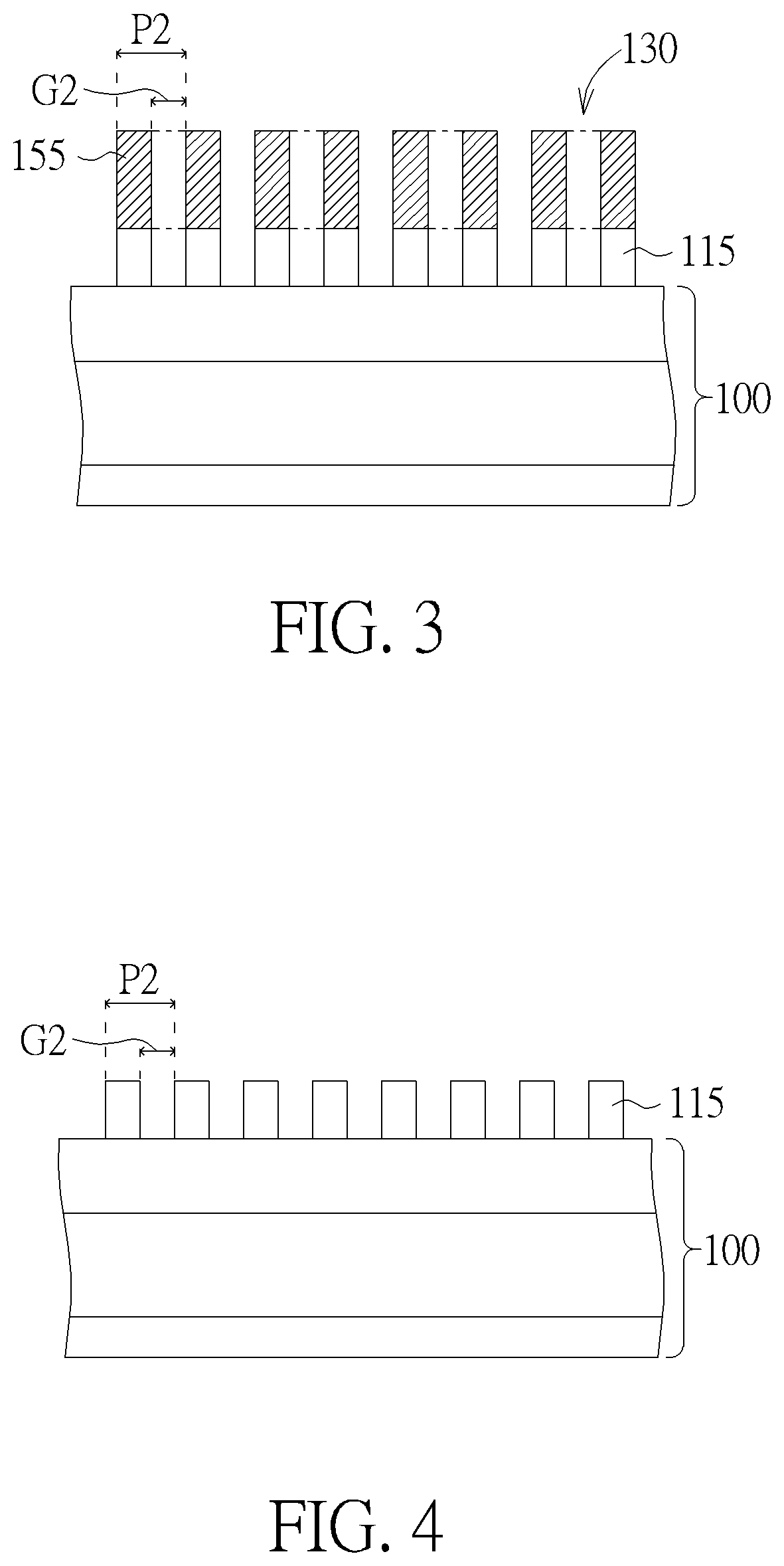
[0021]Please refer to FIG. 1 to FIG. 4, which are schematic diagrams illustrating a forming process of a semiconductor structure according to the present invention. Firstly, a substrate 100 is provided, and a target layer 110 is formed on the substrate 100. The substrate 100 may only include a semiconductor substrate, like a silicon containing substrate, a silicon-on-insulator (SOI) substrate, or includes both of the semiconductor substrate and an insulating layer formed thereon, or includes both of the semiconductor substrate an active element formed therein. In the present embodiment, the target layer 110 for example includes a hard mask layer including a dielectric material like silicon nitride (SiN), silicon oxynitride (SiON) or silicon carbonitride (SiCN), but is not limited thereto. In another embodiment, the target layer 110 may also include a semiconductor layer like a silicon layer or an epitaxial silicon layer, a conductive layer like an aluminum (Al) layer, a copper (Cu) ...

second embodiment

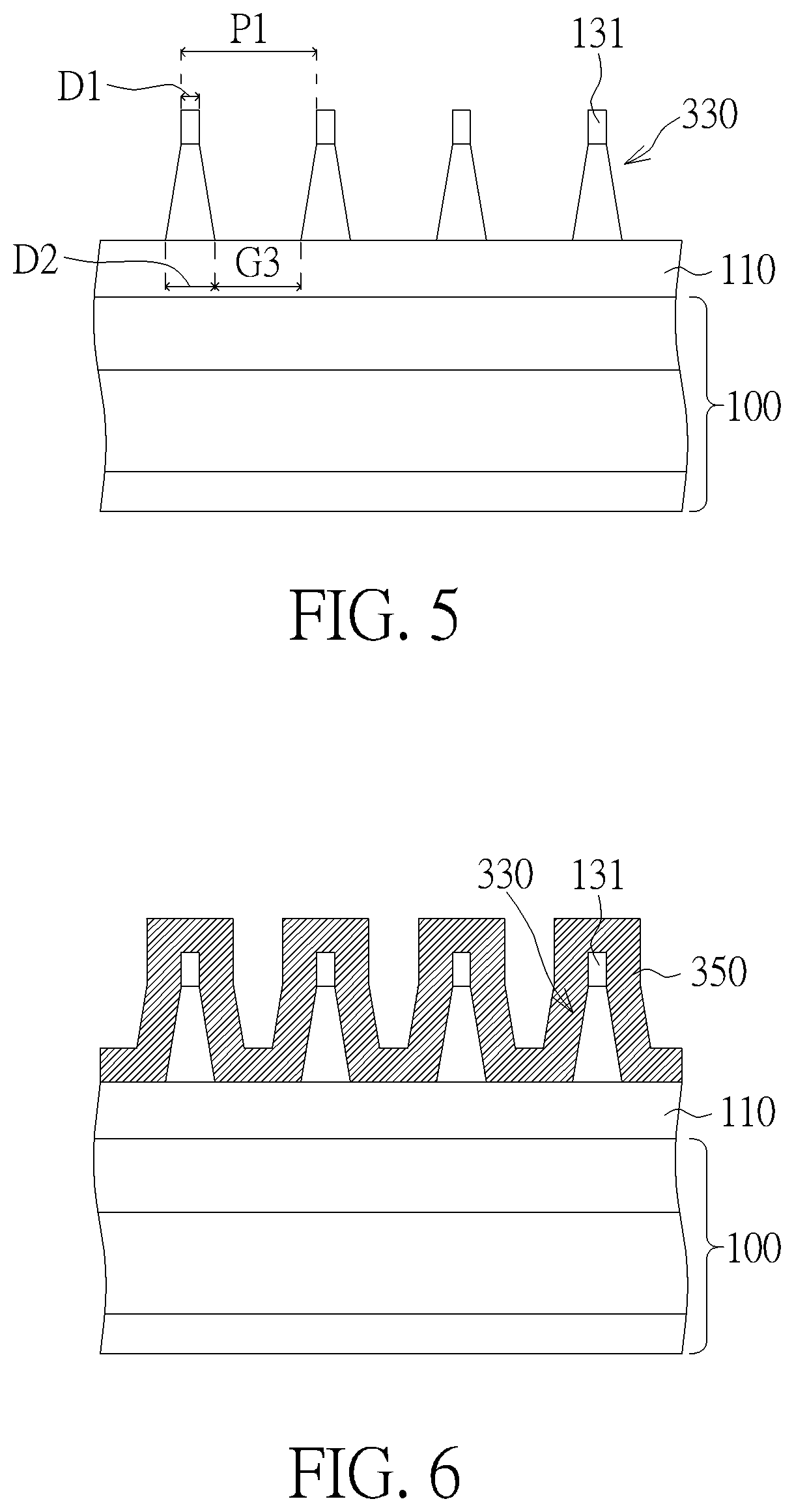
[0036]According to the above steps, a forming process of a semiconductor structure according to the present invention is completed. In the present embodiment, although the SIT technique is still used to form the target patterns 117 or other target structures, the target layer 110 is namely patterned by using a mask formed together from a portion of each mandrel 330 and a portion of the spacer material layer 350 covering on each mandrel 330. That is, each of the target patterns 117 is formed according to one spacer portion 355 and one unetched portion 335 in contact with each other. Thus, the target patterns 117 of the present embodiment may therefore obtains an enlarged dimension, in comparison with the target patterns 115 only formed through the spacers 155. In one embodiment, a dimension of the target patterns 117 is substantially the same or greater than the dimension D2 of the mandrels 330. In this way, the forming process of the present embodiment is allowable to form target st...


PUM

PropertyMeasurementUnit
sizeaaaaaaaaaa
semiconductor structureaaaaaaaaaa
semiconductoraaaaaaaaaa

Abstract

The present invention provides a method of forming a semiconductor structure including the following steps. Firstly, a target layer is formed on a substrate, and a plurality of mandrels is formed on the target layer. Next, a material layer is formed on the target layer to cover the mandrels. Then, an etching process is performed to partially remove each of the mandrel and the material layer covered on each mandrel, to form a plurality of mask. Finally, the target layer is patterned through the masks, to form a plurality of patterns. Through the present invention, each mask comprises an unetched portion of each mandrel and a spacer portion of the material covered on each mandrel, and a dimension of each of the patterns is larger than a dimension of each of the mandrel.

Description

BACKGROUND OF THE INVENTION1. Field of the Invention[0001]The present invention relates to a method of forming semiconductor structure, and more particularly, to a method of forming semiconductor structure by using a self-aligned double patterning (SADP) process for transferring patterns.2. Description of the Prior Art[0002]Fabrication of microstructures requires tiny elements of precisely controlled size formed in a material layer of an appropriate substrate such as semiconductor substrate / layers, dielectric layers and / or metal layers. These tiny elements are generated by patterning the abovementioned substrate / layers, for instance, by performing photolithography and etching processes. For these purposes, in conventional semiconductor techniques, a mask layer is formed on the target, and these tiny elements are defined in the mask layer and followed by being transferred to the target layer. Generally, the mask layer may include or is formed by means of a layer of photoresist that i...

Claims


Application Information

Patent Timeline
Patent Type & Authority Patents(United States)
IPC IPC(8): H01L21/033H01L21/311
CPCH01L21/31116H01L21/0337H01L21/0334
Inventor LIN, GANG-YICHANG, FENG-YILIN, YING-CHIHLEE, FU-CHE
Owner UNITED MICROELECTRONICS CORP
Learn More