Liquid crystal on silicon display and a method of forming the same
- Summary
- Abstract
- Description
- Claims
- Application Information
AI Technical Summary
Benefits of technology
Problems solved by technology
Method used
Image
Examples
Embodiment Construction
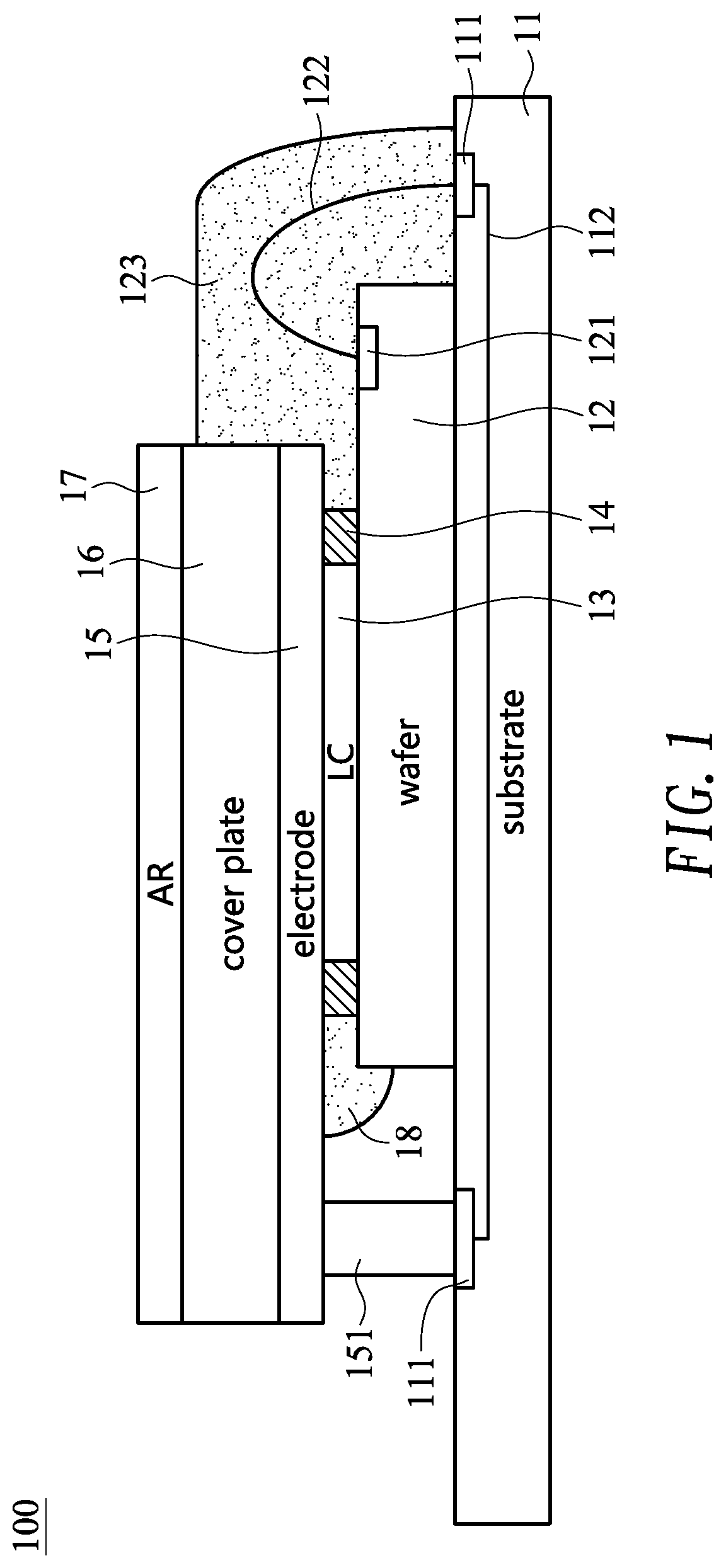
[0009]FIG. 1 shows a cross-sectional view illustrating a liquid crystal on silicon (LCOS) display 100 according to one embodiment of the present invention. It is appreciated that only components pertinent to the embodiment are depicted.
[0010]In the embodiment, the LCOS display 100 may include a substrate 11 such as a printed circuit board (PCB), a flexible printed circuit (FPC) board or a semiconductor (e.g., silicon) substrate. A plurality of (first) bond pads 111 may be disposed on a top surface of the substrate 11, and some of the bond pads 111 may be electrically coupled through wires 112 disposed in or on the substrate 11.
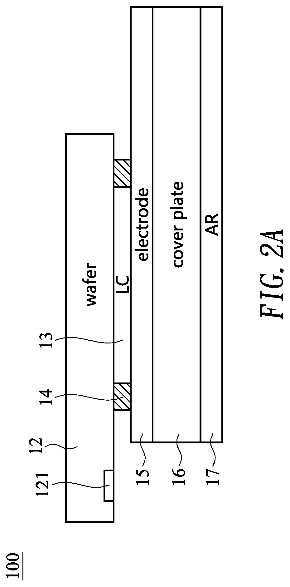
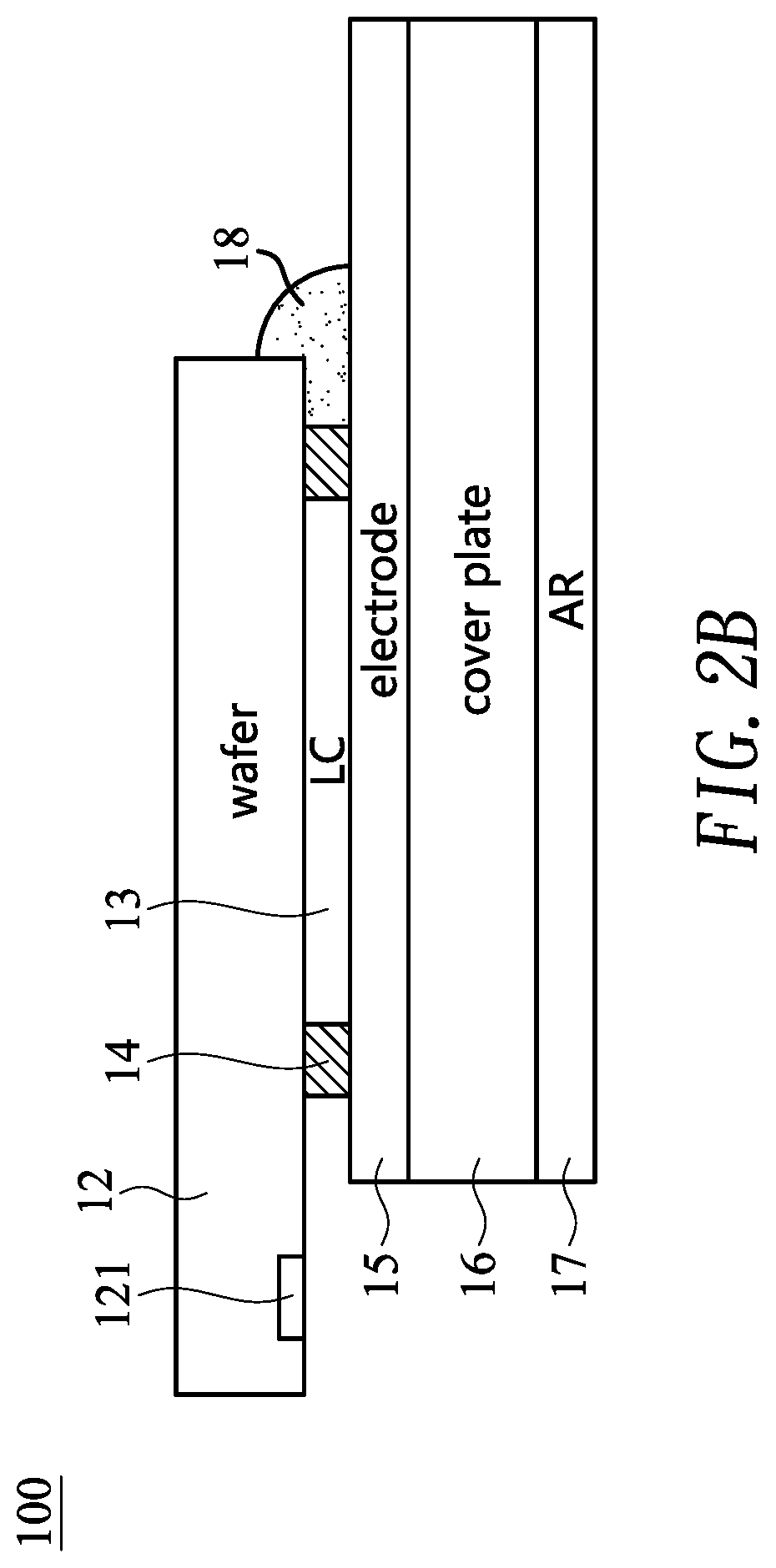
[0011]The LCOS display 100 of the embodiment may include a wafer 12 (e.g., semiconductor wafer such as silicon wafer) disposed on the top surface of the substrate 11, for example, by flip chip bonding. The wafer 12 may include pixel electrodes (not shown) for active-matrix circuits, disposed on a top surface of the wafer 12. At least one (second) bond pad 121 ...
PUM
 Abstract
Description
Claims
Application Information
 - R&D
- Intellectual Property
- Life Sciences
- Materials
- Tech Scout
- Unparalleled Data Quality
- Higher Quality Content
- 60% Fewer Hallucinations
Browse by: Latest US Patents, China's latest patents, Technical Efficacy Thesaurus, Application Domain, Technology Topic, Popular Technical Reports.
© 2025 PatSnap. All rights reserved.Legal|Privacy policy|Modern Slavery Act Transparency Statement|Sitemap|About US| Contact US: help@patsnap.com


