Dielectric electro-optic phase shifter

a dielectric electrooptic and phase shifter technology, applied in non-linear optics, instruments, optics, etc., can solve the problems of limited bandwidth, high optical loss, high power consumption, etc., and achieve low vl, low power consumption, and high operation bandwidth

Active Publication Date: 2021-01-19
COMS IP HLDG LLC
View PDF14 Cites 2 Cited by
  • Summary
  • Abstract
  • Description
  • Claims
  • Application Information

AI Technical Summary

Benefits of technology

[0013]For the present invention, a set of optimizations involving intrinsic and extrinsic properties of both the SRN core and the silicon electrodes is provided. This is done in order to achieve low VπLπ, high bandwidth of operation, and low power consumption, where Vπ and Lπ refer to the voltage and length required to induce a n phase shift. In accordance with the present invention, there are essentially five requirements for an EO phase shifter. These requirements are: i) high optical confinement; ii) high overlap integral; iii) low relative permittivity, εr; iv) high EO coefficient; and v) high electric breakdown strength.
[0014]The first requirement is a high degree of confinement of the optical mode in the EO material. As envisioned for the present invention the optical wave is preferably guided in its fundamental mode. Specifically, for the present invention, the electrodes are made of a P or N doped silicon having a higher index of refraction than that of the SRN core. The surrounding dielectrics will also have a much lower index of refraction. Optimally, the SRN core index of refraction is kept between 2.5 and 3.5 for an operational wavelength λ for the optical wave in a range between 800 and 1,600 nm, to allow for a high degree of confinement. The purpose of this refractive index mismatch is to guide a suitably polarized optical mode into the lower index SRN. Finally, the width W and thickness H of the waveguide core need to be dimensionally selected to further optimize confinement. High confinement minimizes optical loss from interaction of the optical mode with free carriers in the silicon electrodes.
[0016]Thirdly, the SRN core is fabricated to possess a low relative permittivity, εr<10. This ensures a low device capacitance, a high bandwidth of operation, and low energy consumption during device operation.
[0018]Fifthly, in order to get a large change in refractive index, a high electric field is essential. In the case of the present invention, the SRN core is fabricated to have a high electric breakdown strength, EBD>1×10⁸ V / m, with minimal defect density for the thickness H. This is needed to ensure low scattering optical loss and to sustain the high electric field without reliability degradation.

Problems solved by technology

These variants suffer from drawbacks including, but not limited to, high optical losses, high-power consumption, and limited bandwidth because of large device capacitances.
It is known, however, that silicon and the dielectrics available in the CMOS process do not have any second order susceptibility χ(2).
Ergo, the Pockels effect is impractical.
Integration of such materials into silicon photonics platforms has the fundamental drawback of relying on materials and tooling not available within industry standard CMOS process flows.
Additionally, such approaches rely on waveguide structures or configurations that suffer from poor confinement of the optical field in the electro-optic (EO) material, leading to inefficient devices.
However, this approach suffers from an overall low realizable nonlinear coefficient and hence devices which are impractical.
While compatible with CMOS processes, this approach suffers from relatively low electric breakdown strength (EBD)˜4×10⁷ V / m and low χ(3)˜2×10⁻¹⁹ m2 / V2 of silicon.
This, in turn, reduces the strength of the electric field in the intrinsic region, which further causes a degradation in the phase-shifting efficiency of the device.

Method used


Image

  • Dielectric electro-optic phase shifter
  • Dielectric electro-optic phase shifter
  • Dielectric electro-optic phase shifter

Examples


Embodiment Construction

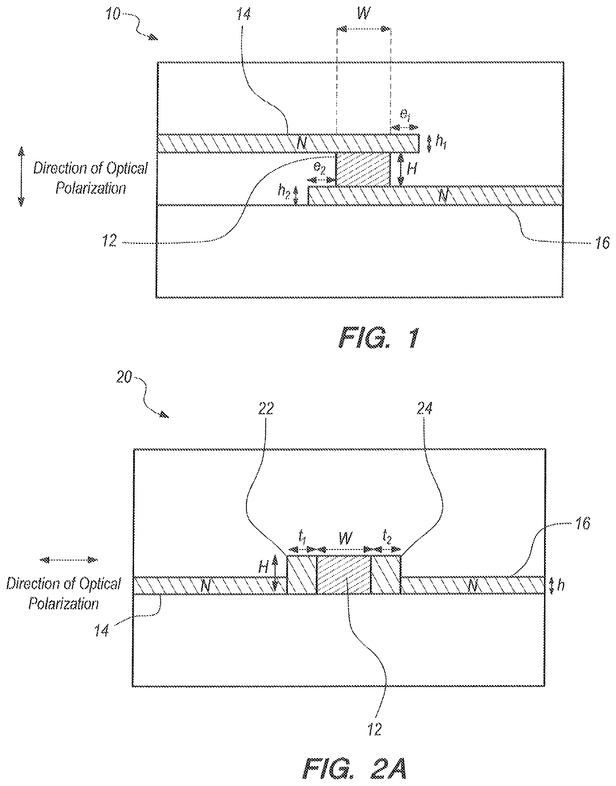
lass="d_n">[0027]Referring initially to FIG. 1, a vertical electro-optic (EO) phase shifter in accordance with the present invention is shown and is generally designated 10. As shown the vertical EO phase shifter 10 includes a waveguide core 12 which is directly connected in intimate contact with a first electrode 14 and a second electrode 16. For the present invention, the waveguide core 12 is made of a Silicon-Rich Silicon Nitride (SRN), while both the first electrode 14 and the second electrode 16 are made of a doped silicon. For purposes of the present invention the first electrode 14 and the second electrode 16 can be either P doped or N doped silicon.

[0028]In detail, the waveguide core 12 is manufactured in a multi-step process involving a silicon-rich silicon nitride (SixNy) film that is deposited by well known Chemical Vapor Deposition (CVD) techniques. These techniques allow for the deposition of a non-stoichiometric silicon nitride film which is silicon rich. In this manne...


PUM

PropertyMeasurementUnit
phase shifting lengthaaaaaaaaaa
relative permittivity εraaaaaaaaaa

Abstract

An EO phase shifter for modulating an electrical signal onto an optical wave is manufactured using CMOS process tools whereby a waveguide core made of EO material has intimate contacts with its electrodes. Specifically, the waveguide core is made of a Silicon-Rich Silicon Nitride (SRN) material which has a high linear refractive index n and a high third order nonlinear susceptibility. The electrodes are made of P or N doped silicon. Also, polarization of the optical wave is oriented normal to interfaces between the waveguide core and the electrodes. With this combination, the EO phase shifter exhibits high optical confinement, low propagation loss, and a high electro-optic overlap integral for modulation.

Description

FIELD OF THE INVENTION[0001]The present invention pertains generally to electro-optic (EO) phase shifters for modulating an optical wave with an electrical signal. In particular, the present invention pertains to electro-optic phase shifters that can be fabricated using standard tooling used in Complementary Metal-Oxide Silicon (CMOS) manufacturing process flows. The present invention is particularly, but not exclusively, useful as an EO phase shifter having a Silicon-Rich Silicon Nitride (SRN) waveguide core that establishes a high overlap integral between the applied electric field E and the optical wave for modulation of the optical wave.BACKGROUND OF THE INVENTION[0002]Electro-optic phase-shifters are known in the prior art. Essentially, they involve using an electrical signal to modulate the phase of a propagating optical wave. This is done via means of modulating the refractive index of the medium which induces a change in phase of the optical wave.[0003]In the field of integr...

Claims


Application Information

Patent Timeline
Patent Type & Authority Patents(United States)
IPC IPC(8): G02F1/025G02F1/035
CPCG02F1/025G02F1/035G02F2203/20G02F2203/50
Inventor SHARMA, RAJATSUN, CHEN-KUOWELSTAND, ROBERT B.
Owner COMS IP HLDG LLC
Why Eureka
Try Eureka