

Multiple electron beam image acquisition apparatus, and alignment method of multiple electron beam optical system
a technology of electron beam and image acquisition apparatus, which is applied in image enhancement, instruments, image data processing, etc., can solve the problems of reducing the yield of lsi manufacturing, beam blur and distortion, and extremely small dimensions of pattern defects needed to be detected
- Summary
- Abstract
- Description
- Claims
- Application Information
AI Technical Summary
Benefits of technology
Problems solved by technology
Method used
Image

Examples
first embodiment
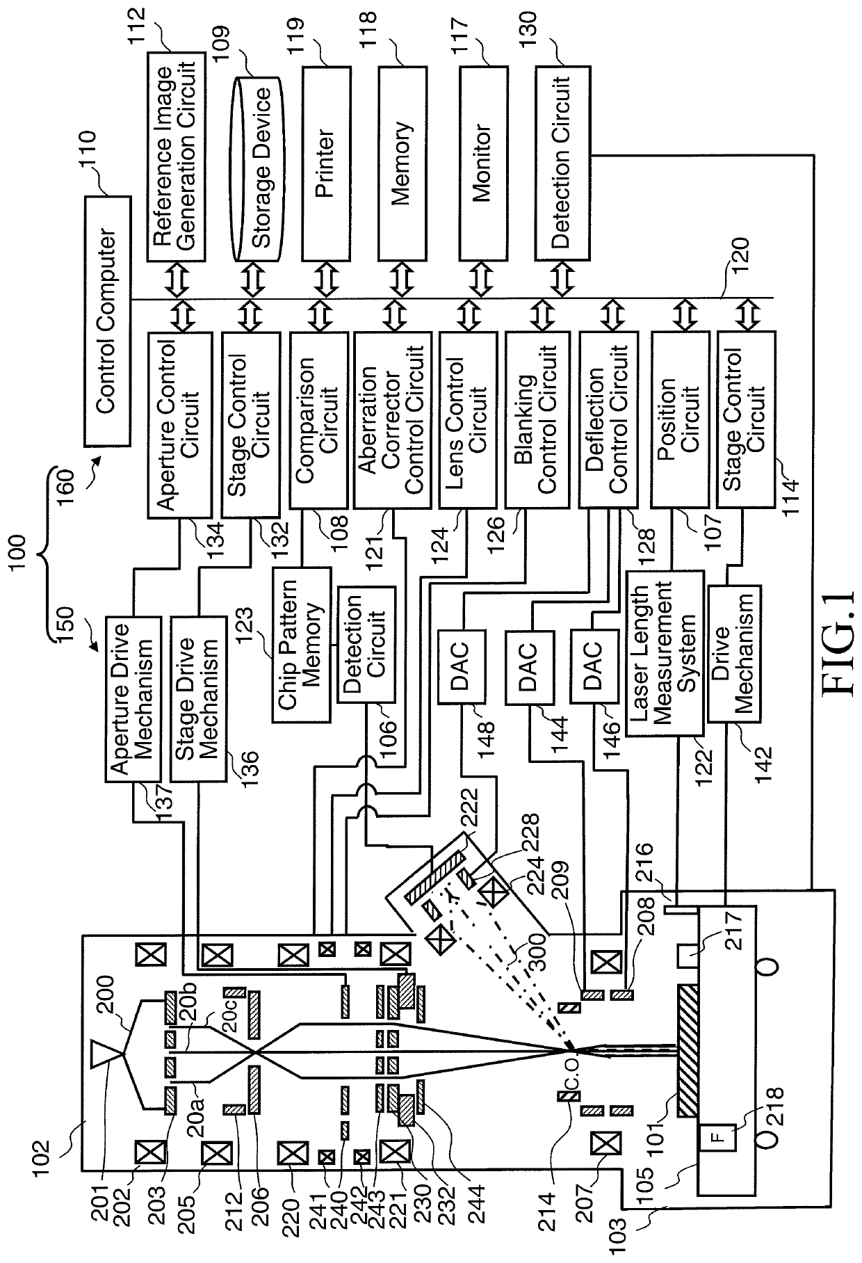
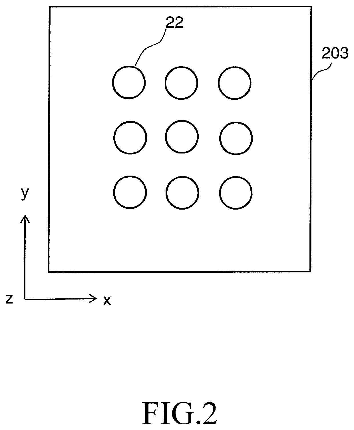
[0033]FIG. 1 shows a configuration of a pattern inspection apparatus according to a first embodiment. In FIG. 1, an inspection apparatus 100 for inspecting patterns formed on the substrate is an example of a multiple electron beam inspection apparatus. The inspection apparatus 100 includes an image acquisition mechanism 150 and a control system circuit 160. The image acquisition mechanism 150 includes an electron beam column 102 (also called an electron optical column) (an example of a multi-beam column), an inspection chamber 103, a detection circuit 106, a chip pattern memory 123, a stage drive mechanism 142, a laser length measuring system 122, a stage drive mechanism 136, and an aperture drive mechanism 137. In the electron beam column 102, there are arranged an electron gun 201, an illumination lens 202, a shaping aperture array substrate 203, an electromagnetic lens 205, a common blanking deflector 212, a limiting aperture substrate 206, an electromagnetic lens 220, an alignme...
PUM
| Property | Measurement | Unit |
|---|---|---|
| acceleration voltage | aaaaa | aaaaa |
| bias potential | aaaaa | aaaaa |
| acceleration voltage | aaaaa | aaaaa |
Abstract
Description
Claims
Application Information