
Electricity measuring type surface plasmon resonance sensor and electricity measuring type surface plasmon resonance sensor chip used in the same

a technology of surface plasmon resonance and electricity, which is applied in the direction of material analysis, phase-affecting property measurement, instruments, etc., can solve the problems of high throughput, difficult integration, and large size of the apparatus, and achieves easy reduction in size, high throughput, and sufficient sensor accuracy

Active Publication Date: 2021-04-20
IMURA JAPAN +1
View PDF17 Cites 1 Cited by
  • Summary
  • Abstract
  • Description
  • Claims
  • Application Information

AI Technical Summary

Benefits of technology

The present invention is about a new type of electricity measuring surface plasmon resonance sensor that is small, efficient, and accurate. This patent is also about a specific chip used for this new sensor. Overall, this invention provides a solution for measuring electricity with a high throughput.

Problems solved by technology

However, since it is necessary to use an optical system to detect the change in surface plasmon resonance angle due to the change in the concentration of the target substance present on the metal surface, the sensor chip as described in PTL 1 has problems that the apparatus tends to be expensive or large in size and that it is difficult to achieve integration and a higher throughput achieving processing a large number of samples at the same time.
However, since the absorbance of the light transmitted between the metal fine particles is measured to detect the change in the refractive index of the medium in the vicinity of the surfaces of the metal fine particles due to adsorption or deposition of the target substance on the metal fine particles, the localized plasmon resonance sensor described in PTL 2 has problems that it is necessary to precisely control the size and arrangement of the metal fine particles and that it is difficult to sufficiently enhance the intensity of the detection signal because the detection signal is the absorbance.

Method used


Image

  • Electricity measuring type surface plasmon resonance sensor and electricity measuring type surface plasmon resonance sensor chip used in the same
  • Electricity measuring type surface plasmon resonance sensor and electricity measuring type surface plasmon resonance sensor chip used in the same
  • Electricity measuring type surface plasmon resonance sensor and electricity measuring type surface plasmon resonance sensor chip used in the same

Examples


example 1

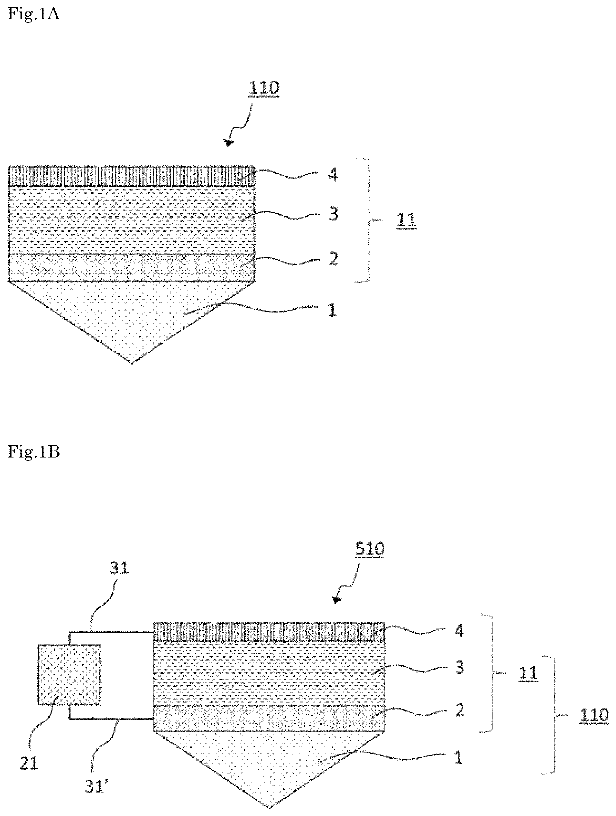
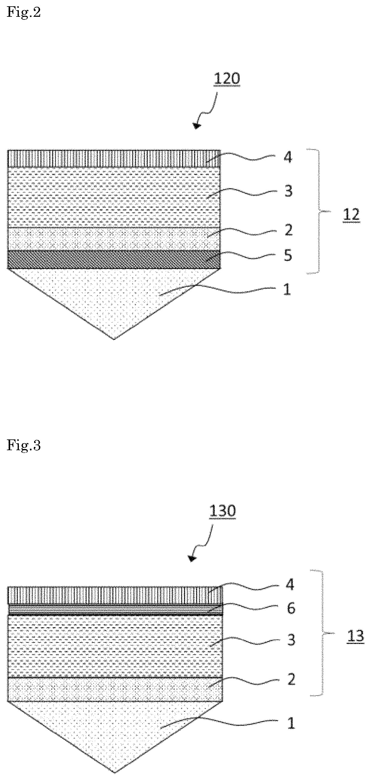
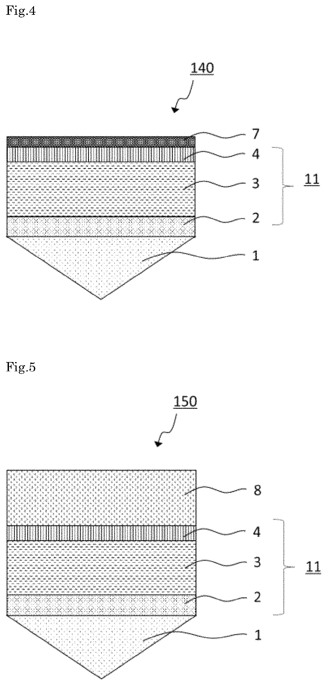
[0113]A chip (photoelectric conversion unit (sensor chip)) formed by stacking the glass substrate, the ITO film, the TiO2 film, and the Au film in this order was obtained in the same manner as that of Comparative Example 1. Next, the surface of the glass substrate of the obtained element opposite to the ITO film was coated with 1.5 μL of 80% glycerol and was brought into close contact with the inclined face of the right-angled prism (BK-7 Right-Angled Prism PS908, isosceles right triangle, manufactured by Thorlabs, Inc., refractive index: 1.51) to obtain a chip formed by stacking the prism, the glycerol, the glass substrate, the ITO film, the TiO2 film, and the Au film in this order (prism-attached chip). FIG. 7 illustrates a scanning electron micrograph obtained by observing a longitudinal cross-section of the chip obtained in Example 1 (the glass substrate (the transparent substrate 5), the ITO film (the transparent electrode 2), the TiO2 film (the n-type transparent semiconductor...

example 2

[0123]A chip (prism-attached chip) formed by stacking a prism, diiodomethane, a glass substrate, an ITO film, a TiO2 film, and an Au film (thickness: 50 nm) in this order was obtained in the same manner as that of Example 1 except that right-angled prism S-TIH11 (manufactured by OHARA Inc., refractive index: 1.77) was used instead of BK-7 Right-Angled Prism and 0.5 μL of diiodomethane (first grade, manufactured by FUJIFILM Wako Pure Chemical Corporation) was coated instead of 1.5 μL of 80% glycerol.

example 3

[0124]A chip (prism-attached chip) formed by stacking a prism, diiodomethane, a glass substrate, an ITO film, a TiO2 film, and an Au film (thickness: 30 nm) in this order was obtained in the same manner as that of Example 2 except that the thickness of the Au film was changed to 30 nm in the chip (photoelectric conversion unit (sensor chip)) formed by stacking a glass substrate, an ITO film, a TiO2 film, and an Au film in this order.


PUM

PropertyMeasurementUnit
thicknessaaaaaaaaaa
diameteraaaaaaaaaa
diameteraaaaaaaaaa

Abstract

An electricity measuring type surface plasmon resonance sensor including: a plasmon polariton intensifying sensor chip in which a prism and a sensor chip including a transparent electrode, an n-type transparent semiconductor film, and a plasmon resonance film electrode arranged in this order are arranged in an order of the prism, the transparent electrode, the n-type transparent semiconductor film, and the plasmon resonance film electrode; and an electric measuring apparatus which directly measures a current or voltage from the transparent electrode and the plasmon resonance film electrode.

Description

TECHNICAL FIELD[0001]The present invention relates to an electricity measuring type surface plasmon resonance sensor and an electricity measuring type surface plasmon resonance sensor chip used in the same.BACKGROUND ART[0002]Surface plasmon resonance (SPR) is a state in which free electrons are in collective oscillatory motion (plasma oscillation) on a metal surface, and is classified into propagating surface plasmon resonance (PSPR) which propagates over a metal surface and localized surface plasmon resonance (LSPR) which is localized at a metal structure in nanometer size. The propagating surface plasmon resonance is a state in which resonance is taking place due to the interaction between the incident light and the electric field produced around the free electrons under plasma oscillation, and an electron compression wave (surface plasmon polariton, SPP) formed by the coupling of the plasma oscillation and the electromagnetic wave traveling along the interface propagates along t...

Claims


Application Information

Patent Timeline
Patent Type & Authority Patents(United States)
IPC IPC(8): G01N21/552G01N21/41H01L31/0232H01L31/108
CPCG01N21/553G01N21/41H01L31/0232H01L31/108G01N27/129
Inventor SUZUKI, HIRONORIALLISON, GILESSASAKI, MASANORIHAYASHI, KOKIMISAWA, HIROAKIUENO, KOSEI
Owner IMURA JAPAN
Learn More