
High-χ block copolymers for directed self-assembly

a high- block, self-assembly technology, applied in the field of polymers, can solve the problems of increasing manufacturing cost and complication, increasing manufacturing cost, and increasing the difficulty of conventional photolithography techniques, and achieve the effect of facilitating alignment and surface energy

Active Publication Date: 2021-08-03
BREWER SCI
View PDF19 Cites 0 Cited by
  • Summary
  • Abstract
  • Description
  • Claims
  • Application Information

AI Technical Summary

Benefits of technology

[0080]One advantage of the present invention is that, in embodiments where a hardmask neutral layer is utilized, the surface properties of that layer can be modified from a neutral layer that will facilitate aligning of the self-assembling materials to a non-alignment layer over which the self-assembling materials will not align during annealing or self-assembly. One possible avenue for modifying the hardmask layer involves chemoepitaxy. A stack is prepared comprising a substrate, optional intermediate layer, hardmask neutral layer, and imaging layer, as described above. A pre-pattern is created in the imaging layer, either using the method described previously, or any other conventional method. Thus, pre-pattern formation results in portions of the hardmask layer underneath the imaging layer being uncovered or exposed when those selected portions of the imaging layer are removed from the stack. The remaining portions of the imaging layer adjacent the hardmask serve as a mask for surface modification of the hardmask neutral layer. In one or more embodiments, the imaging layer is patterned using optical lithography and a developer (e.g., alkaline developer) or solvent rinse. Alternatively, the imaging layer is patterned using another suitable method, followed by contact with a developer solution (e.g., alkaline developer) or solvent. Regardless, the exposed portions of the hardmask layer are contacted with a developer solution (separately or during developer rinse). The remaining portions of the imaging layer are then removed (e.g., with solvent), yielding the hardmask layer having surface-modified regions and non-modified regions, where the surface-modified regions correspond to those portions of the hardmask that were uncovered during patterning of the imaging layer. Advantageously, contact with the developer (and particularly with an alkaline developer) changes the surface energy of the hardmask layer. In one or more embodiments, the surface energy is increased and causes the surface-modified regions of the hardmask to lose their ability to act as a neutral layer and induce alignment during the self-assembly process. However, the non-modified regions of the hardmask, which remained covered by the imaging layer during patterning and developer contact, still retain their neutral layer properties. Thus, the surface-modified regions correspond to non-aligning areas while the non-modified regions correspond to aligning areas on the hardmask. The active aligning areas therefore have the ability to become guiding structures for pattern formation during self-assembly.
[0081]A DSA layer is then formed directly on top of the surface-modified hardmask layer, such that there is direct contact between the DSA layer and surface-modified regions and non-modified regions. The DSA layer is then self-assembled as described above to allow the components to self-assemble. Because of the surface modification, the self-assembling layer will only self-assemble into first self-assembled regions and second self-assembled regions in those portions of the DSA layer that are adjacent the non-modified areas of the hardmask. In other words, portions of the DSA layer adjacent the surface-modified areas of the hardmask do not separate or segregate into a pattern during annealing or self-assembly and are “unassembled” or “non-aligned.” One of the first or second self-assembled regions can then be selectively removed, followed by etching the resulting pattern into the hardmask layer and optional intermediate layer. This pattern is eventually transferred down into the substrate.
[0082]In embodiments where a hardmask neutral layer is not utilized, an intermediate layer is required that will form modified and non-modified areas or regions, and the rest of the process would proceed as described above. In a further embodiment, this intermediate layer could be patterned directly, thus avoiding the need to use an imaging or photoresist layer that must ultimately be removed. That is, selective exposure to radiation will result in the creation of the surface-modified areas or regions noted above.
[0083]It will be appreciated that in each of the foregoing methods, self-assembly or annealing results in nanophase separation in the DSA layer, which permits the formation of nanometer-sized patterns (e.g., 10 nm or even sub-10 nm) generally not achievable using conventional optical lithography techniques. It will also be appreciated that although the present methods illustrate formation of at least two distinct annealed or self-assembled regions in the DSA layer, it is envisioned that additional DSA materials could be formulated that are capable of separation into more than two distinct phases, including third and fourth annealed or self-assembled regions.EXAMPLES
[0084]The following examples set forth preferred methods in accordance with the invention. It is to be understood, however, that these examples are provided by way of illustration and nothing therein should be taken as a limitation upon the overall scope of the invention.

Problems solved by technology

Conventional photolithography techniques become increasingly difficult and costly as the feature size approaches 22 inn and smaller.
However, high-χ BCPs are generally difficult to direct and orientate their DSA morphologies due to the disparate polarities and properties between blocks.
They need either an extra top-coat layer or solvent annealing to obtain perpendicular orientation, which can greatly increase the manufacturing cost and complication.
This makes incorporating these BCPs into traditional lithographic tracks much more difficult as these are not typical techniques used currently in lithography.

Method used


Image

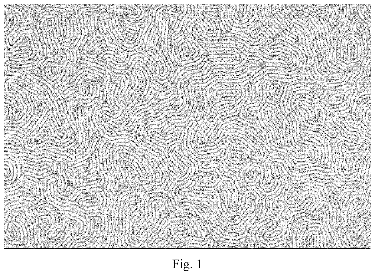
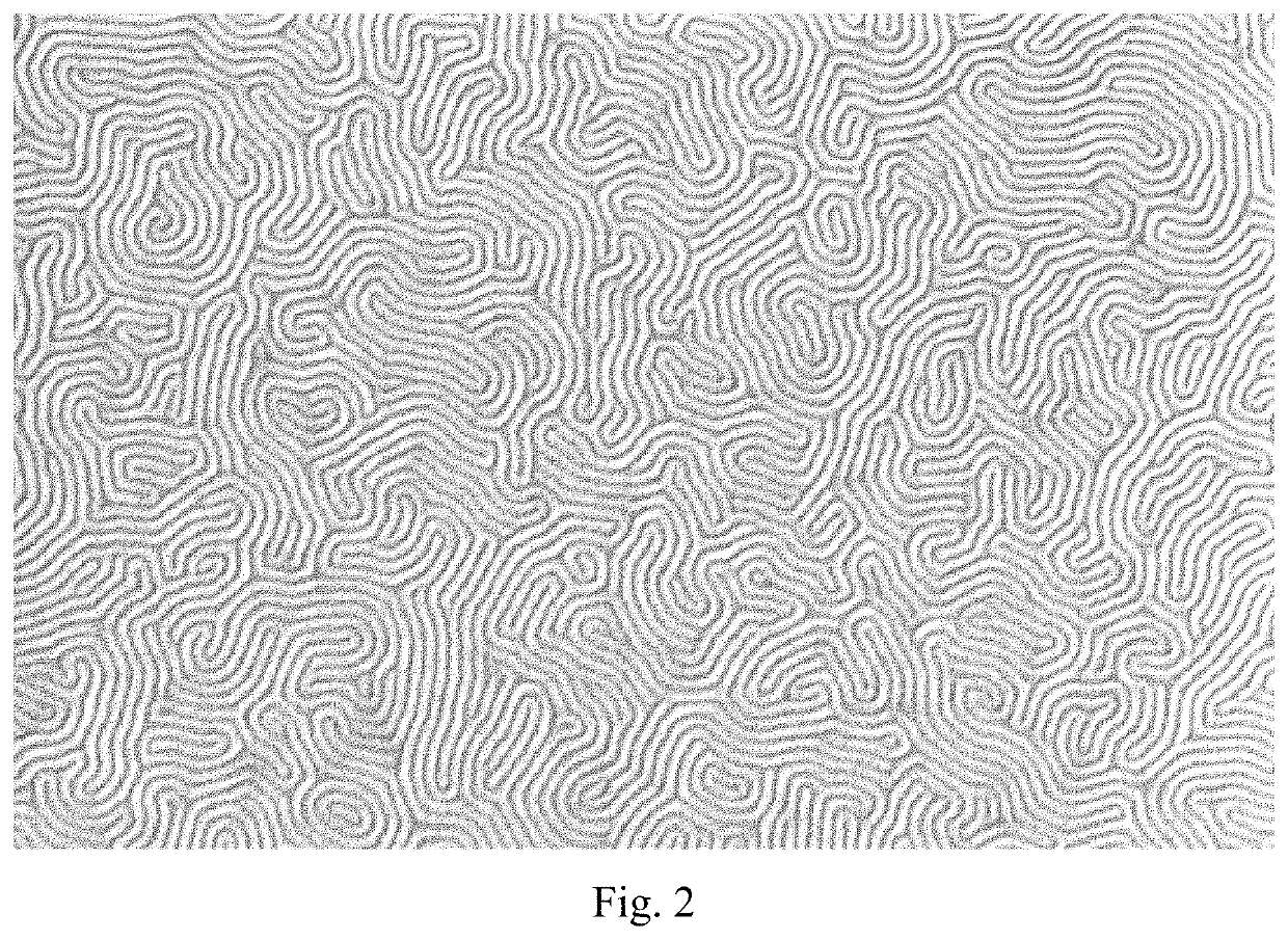
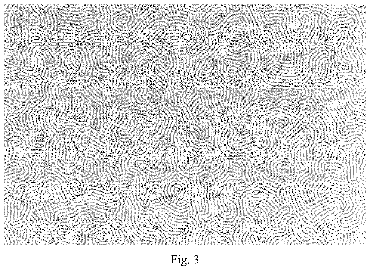
  • High-χ block copolymers for directed self-assembly
  • High-χ block copolymers for directed self-assembly
  • High-χ block copolymers for directed self-assembly

Examples


example 1

Synthesis of P(MMA-r-HEMA)

[0085]Methyl methacrylate (19.02 g, Sigma Aldrich, St. Louis, Mo.), 2-hydroxyethyl methacrylate (1.30 g, Sigma Aldrich, St. Louis, Mo.), 2-cyano-2-propyl benzodithioate (0.161 g, Strem Chemicals Inc., Newburyport, Mass.), 2,2′-azobis(2-methylpropionitrile) (0.015 g, Sigma Aldrich, St. Louis, Mo.), and ethyl acetate (30 g, Alfa Aesar, Ward Hill, Mass.) were added to a round bottom flask and purged for 30 minutes with N2. The reaction was heated at 60° C. for 16 hours before being cooled to room temperature, diluted with acetone (Sigma Aldrich, St. Louis, Mo.) and precipitated into hexanes (450 mL, Alfa Aesar, Ward Hill, Mass.). The resulting powder was collected by vacuum filtration and dried under vacuum overnight at 45° C. Finally, 10.8 grams of P(MMA-r-HEMA) was collected and analyzed by GPC to be 13.1 kg / mol relative to PS standards with a PDI of 1.07.

example 2

Chain Extension with Styrene

[0086]In this procedure, 1.6 grams of 13.1k P(MMA-r-HEMA) from Example 1 was mixed with 9.37 grams of styrene (TCI America, Portland, Oreg.), 4.2 milligrams of 2,2′-azobis(2-methylpropionitrile) (Sigma Aldrich, St. Louis, Mo.), and 9 grams of toluene (Sigma Aldrich, St. Louis, Mo.). The solution was purged with N2 for 30 minutes and heated to 80° C. for 16 hours before being cooled to room temperature, diluted with acetone (Sigma Aldrich, St. Louis, Mo.), and precipitated into a 2:1 (v / v) mixture of cyclohexane (Alfa Aesar, Ward Hill, Mass.) to hexanes (Alfa Aesar, Ward Hill, Mass.). The resulting powder was collected by vacuum filtration and dried under vacuum overnight at 45° C. Finally, 3.0 grams of P(MMA-r-HEMA)-b-PS was collected and analyzed by GPC to be 31.8 kg / mol relative to PS standards with a PDI of 1.12.

example 3

Chain Extension with Styrene, 4-Vinylbiphenyl, and 4-Methylstyrene

[0087]In this Example, 1.6 grams of 13.1k P(MMA-r-HEMA) from Example 1 was mixed with 2.58 grams of styrene (TCI America, Portland, Oreg.), 1.98 grams of 4-vinylbiphenyl (Proactive Molecular Research, Alachua, Fla.), 2.27 grams of 4-methylstyrene (Sigma Aldrich, St. Louis, Mo.), 4.2 milligrams of 2,2′-azobis(2-methylpropionitrile) (Sigma Aldrich, St. Louis, Mo.), and 9 grams of toluene (Sigma Aldrich, St. Louis, Mo.). The solution was purged with N2 for 30 minutes and heated to 80° C. for 16 hours before being cooled to room temperature, diluted with acetone (Sigma Aldrich, St. Louis, Mo.) and precipitated into a 2:1 (v / v) mixture of cyclohexane (Alfa Aesar, Ward Hill, Mass.) to hexanes (Alfa Aesar, Ward Hill, Mass.). The resulting powder was collected by vacuum filtration and dried under vacuum overnight at 45° C. Finally, 3.1 grams of P(MMA-r-HEMA)-b-P(S-r-VBP-r-4-methylstyrene) was collected and analyzed by GPC to ...


PUM

PropertyMeasurementUnit
polydispersity indexaaaaaaaaaa
Tgaaaaaaaaaa

Abstract

The present invention is broadly concerned with novel directed self-assembly compositions, processes utilizing those compositions, and the resulting structures that are formed. The composition comprises a block copolymer of polystyrene and a polymethylmethacrylate block with polylactic acid side chains (“PS-b-P(MMA-LA)”). The block copolymer is capable of crosslinking and micro-phase separating into lines and spaces measuring about 10-nm or smaller with sub-20 nm L0 capability. Additionally, PS-b-P(MMA-LA) can be thermally annealed without a top-coat for simpler processing than the prior art. The polylactic acid side chains also increase the etch rate of the poly(methylmethacrylate) block when exposed to oxygen plasma, as well as lower the Tg.

Description

RELATED APPLICATION[0001]The present application claims the priority benefit of U.S. Provisional Patent Application Ser. No. 62 / 433,996, filed Dec. 14, 2016, entitled HIGH-CHI BLOCK COPOLYMERS FOR DIRECTED SELF-ASSEMBLY, incorporated by reference in its entirety herein.BACKGROUND OF THE INVENTIONField of the Invention[0002]This invention pertains to polymers for use in the block copolymer materials used in directed self-assembly.Description of the Prior Art[0003]The increasing demand of smaller micro-fabricated devices requires a continuous decrease in the feature size of device components. Conventional photolithography techniques become increasingly difficult and costly as the feature size approaches 22 inn and smaller. To keep Moore's law moving forward, non-lithography techniques will become more and more important. An alternative approach to generate nanoscale patterns is directed self-assembly (“DSA”) of block copolymers (“BCPs”), which can feasibly provide highly-ordered, patt...

Claims


Application Information

Patent Timeline
Patent Type & Authority Patents(United States)
IPC IPC(8): C08G81/00C08G81/02C08F293/00G03F7/16G03F7/20C08L87/00H01L21/027G03F7/32C08G63/08G03F7/00C08L53/00C08G65/40B32B27/28
CPCC08G81/027B32B27/28C08F293/00C08F293/005C08G63/08C08G65/40C08G81/02C08L53/00C08L87/00C08L87/005G03F7/0002G03F7/16G03F7/20G03F7/327H01L21/0271C08F2438/03C08L2201/56C08L2203/20C08F220/14C08F220/20C08F212/08C08F220/283C08F212/12C08F212/34
Inventor SWEAT, DANIELXU, KUI
Owner BREWER SCI
Learn More