
Compute-in-memory (CIM) employing low-power CIM circuits employing static random access memory (SRAM) bit cells, particularly for multiply-and-accumluate (MAC) operations

a technology of compute-in-memory and bit cells, applied in computing, digital storage, instruments, etc., can solve the problems of voltage flip on the complementary storage node, read disturbance issue between the storage circuit, etc., to reduce the standby and dynamic power of the cim circuit, reduce the supply voltage, and increase the likelihood of a read disturbance

Active Publication Date: 2021-11-16
QUALCOMM INC
View PDF1 Cites 5 Cited by
  • Summary
  • Abstract
  • Description
  • Claims
  • Application Information

AI Technical Summary

Benefits of technology

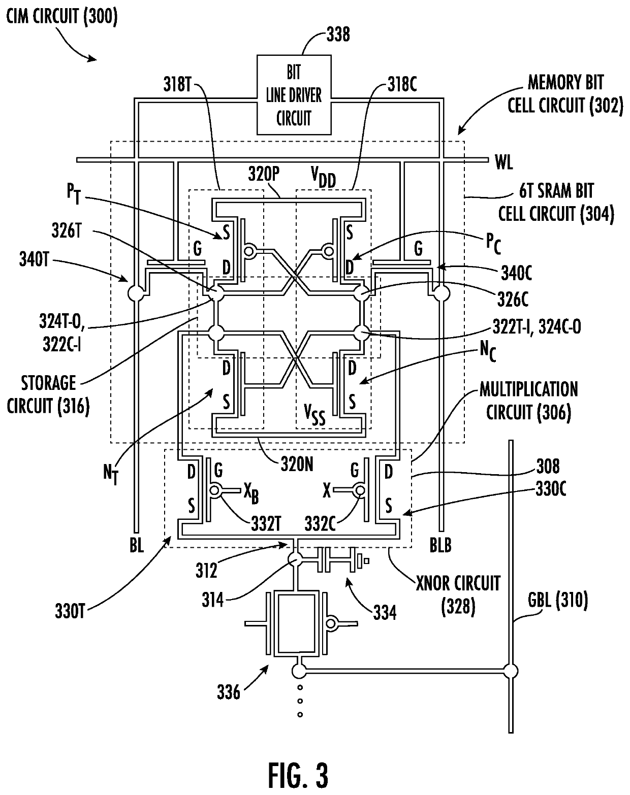
The patent text describes a circuit design for a computer-implemented memory (CIM) system that reduces power consumption and improves performance. The design includes a five-transistor (5T) SRAM bit cell circuit that eliminates a complement access circuit, reducing contention between the two circuits. By eliminating the complement bit line and complement access transistor, dynamic power of the CIM circuit is reduced. The reduced bit line pre-charge voltage in a read operation increases the voltage margin, reducing standby power. However, writing data into the 5T SRAM bit cell circuit can be difficult, so the supply voltage can be boosted to avoid write contention. The CIM system can also include one or more arrays of CIM circuits coupled to a common global bit line, and the distance between the bit line driver circuit and the farthest away CIM circuit in the array can be reduced to reduce line capacitance and dynamic power consumption. Additionally, the global bit line can be pre-charged at a reduced supply voltage to further reduce dynamic power of the CIM circuits.

Problems solved by technology

However, reducing the bit line pre-charge voltage for a read operation can cause a read disturbance issue between the storage circuit and the access circuit of the SRAM bit cell.
This could cause a voltage flip on the complementary storage node.

Method used


Image

  • Compute-in-memory (CIM) employing low-power CIM circuits employing static random access memory (SRAM) bit cells, particularly for multiply-and-accumluate (MAC) operations
  • Compute-in-memory (CIM) employing low-power CIM circuits employing static random access memory (SRAM) bit cells, particularly for multiply-and-accumluate (MAC) operations
  • Compute-in-memory (CIM) employing low-power CIM circuits employing static random access memory (SRAM) bit cells, particularly for multiply-and-accumluate (MAC) operations

Examples


Embodiment Construction

[0029]With reference now to the drawing figures, several exemplary aspects of the present disclosure are described. The word “exemplary” is used herein to mean “serving as an example, instance, or illustration.” Any aspect described herein as “exemplary” is not necessarily to be construed as preferred or advantageous over other aspects.

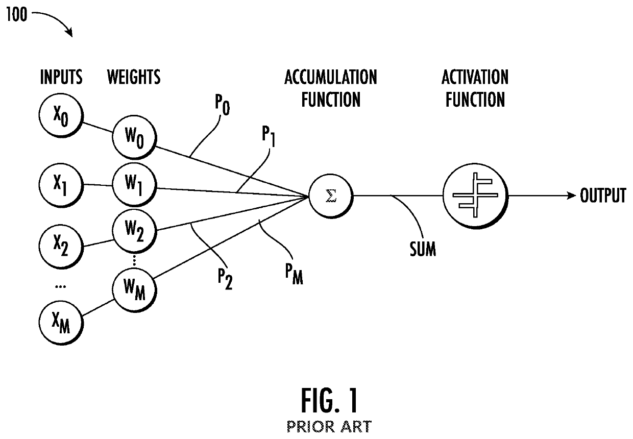
[0030]Aspects disclosed in the detailed description include low-power compute-in-memory (CIM) systems employing CIM circuits employing static random access memory (SRAM) bit cells. As a non-limiting example, the CIM circuits can be used for multiply-and-accumulate (MAC) operations, such as those employed in machine-learning applications. The CIM circuits each include a SRAM bit cell circuit that includes a storage circuit for storing data. Data can be read from the storage circuit of the SRAM bit cell circuit by pre-charging a bit line and activating an access circuit (e.g., an access transistor) coupled between the bit line and the storage circuit. D...


PUM


Abstract

Low-power compute-in-memory (CIM) systems employing CIM circuits that include static random access memory (SRAM) bit cells circuits. The CIM circuits can be used for multiply-and-accumulate (MAC) operations. The CIM circuits can include five-transistor (5T) SRAM bit cells that each have a single bit line coupled to an access circuit for accessing the SRAM bit cell for read / write operations. The CIM circuit also includes a multiplication circuit (e.g., an exclusive OR (XOR)-based circuit) coupled to the SRAM bit cell. The CIM circuit is configured to perform multiplication of an input data value received by the multiplication circuit with a weight data value stored in the SRAM bit cell. The reduction of an access circuit in the 5T SRAM bit cell allows the pull-up voltage at a supply voltage rail coupled to the inverters of the 5T SRAM bit cell to be reduced to reduce standby power while providing storage stability.

Description

BACKGROUNDI. Field of the Disclosure[0001]The technology of the disclosure relates generally to machine learning computing, and more particularly to computational compute-in-memory (CIM) circuits integrated with static random access memory (SRAM) cell circuits for machine learning computing.II. Background[0002]Machine learning is the ability of a computing device to progressively improve performance of a particular task. For example, machine-learning algorithms can use results from processing known data to “train” a computing device to process new data with a higher degree of accuracy. Neural networks are a framework in which machine-learning algorithms may be implemented. A neural network is modeled after the organization of a brain, with a plurality of nodes that each correspond to a brain synapse. Each node receives input signals representing input data from preceding nodes and generates an output that becomes an input signal to succeeding nodes. The nodes are organized in sequen...

Claims


Application Information

Patent Timeline
Patent Type & Authority Patents(United States)
IPC IPC(8): G11C7/00G11C11/4094G11C11/4096G11C5/06G11C11/4074G11C11/404
CPCG11C11/4094G11C5/06G11C11/4045G11C11/4074G11C11/4096G06F7/5443G06F7/523G11C11/54G11C11/412G11C11/419G11C11/418
Inventor SHAIK, KHAJA AHMADCHAVA, BHARANIPATHAN, DAWUTH SHADULKHAN
Owner QUALCOMM INC
Learn More