Reduced visibility conductive micro mesh touch sensor

a micro-mesh touch sensor and visibility reduction technology, applied in the field of touch sensors, can solve the problems of generating specular reflection of incident light, reflecting and distracting the end user, copper or copper alloys in conductive materials, etc., to reduce the percentage of specular reflection of light, reduce the amount of light specular reflection, and increase the scattering of incident light

Active Publication Date: 2022-03-01
FUTURETECH CAPITAL INC
View PDF13 Cites 0 Cited by
  • Summary
  • Abstract
  • Description
  • Claims
  • Application Information

AI Technical Summary

Benefits of technology

[0016]Disclosed embodiments significantly reduce the percentage of specularly reflected light by nanometer scale roughening or texturing of the conductor planar surface. Nano roughening or texturing will increase the amount of scattering of the incident light, thus reducing the amount of light specularly reflected towards the user.
[0017]In some embodiments a method for fabricating a metallic wire mesh touch sensor with reduced visibility is provided. A metallic wire mesh is formed on a transparent substrate such that the surface of the metallic wires is roughened or textured, so as to cause high scattering of incident light, thereby minimizing specularly reflected light towards the user. The metal lines are formed over patterned catalytic photoresist. The rough or textured surface of the metallic wires is achieved by roughening or texturing the catalytic photoresist, by selecting parameters of electroless plating of copper to control the surface roughness of the plated copper, or a combination of both. An RMS surface roughness of about 50 nm would scatter approximately 70% of incident cyan light incident at 30°.

Problems solved by technology

However, there are a number of challenges with highly conductive micro mesh systems, including metallic mesh touch sensors.
For example, a big challenge with metallic mesh touch sensors is visibility to eyes of end users.
At certain angles, in particular under bright lights or outdoors, metallic lines of the conductive mesh touch sensors may be highly reflective and distracting to the end users.
Moreover, the general process of forming the metal mesh naturally leads to the metal lines having a smooth surface finish, which generate specular reflection of incident light.
However, the use of copper or copper alloys in a conductive pattern presents a number of challenges.
In addition, copper or copper alloys are prone to surface oxidation on exposure to ambient conditions and are prone to corrosion in certain environmental conditions.
With respect to reliability and environmental performance metrics, a conductive pattern is prone to degradation from use and other causes overtime.
Depending on the type of degradation, the reliability may be affected by the development of electrical opens or electrical shorts upon continued operation.
However, these layers consume a substantial portion of the copper or copper alloy in the process, potentially decreasing conductivity and increasing resistivity, and potentially become insulators.
However, copper or copper alloy having such a thickness may result in stress, poor adhesion, and other failure modes, especially when deposited by an electroless plating process.
In addition, the copper or copper alloys may be prone to electro-migration.
As such, it is difficult to achieve micrometer-fine feature sizes in conductive patterns comprised of copper or copper alloys.
The other drawback with this method is controlling the thickness uniformity of the oxide or sulfide layer, which in turn affect the reflectance and color of the reflected light.
The non-uniform reflected conductor pattern can be objectionable to the end user.
However, the palladium or nickel has a high reflectance value of greater than 80 percent and does not eliminate or reduce the overall specular reflection under high ambient light.

Method used


Image

  • Reduced visibility conductive micro mesh touch sensor
  • Reduced visibility conductive micro mesh touch sensor
  • Reduced visibility conductive micro mesh touch sensor

Examples


Embodiment Construction

[0032]Embodiments of the inventive metallic mesh touch sensor will now be described with reference to the drawings. Different embodiments or their combinations may be used for different applications or to achieve different benefits. Depending on the outcome sought to be achieved, different features disclosed herein may be utilized partially or to their fullest, alone or in combination with other features, balancing advantages with requirements and constraints. Therefore, certain benefits will be highlighted with reference to different embodiments, but are not limited to the disclosed embodiments. That is, the features disclosed herein are not limited to the embodiment within which they are described, but may be “mixed and matched” with other features and incorporated in other embodiments.

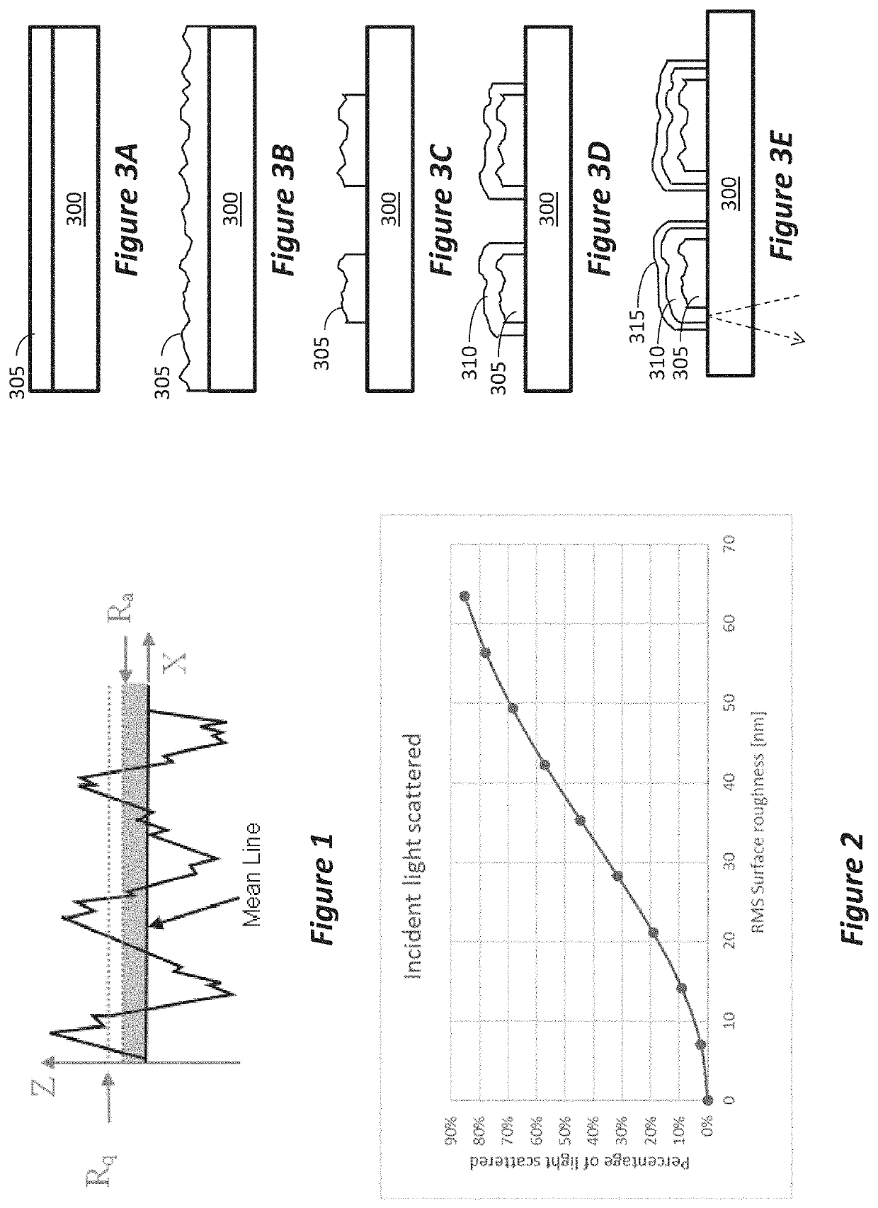
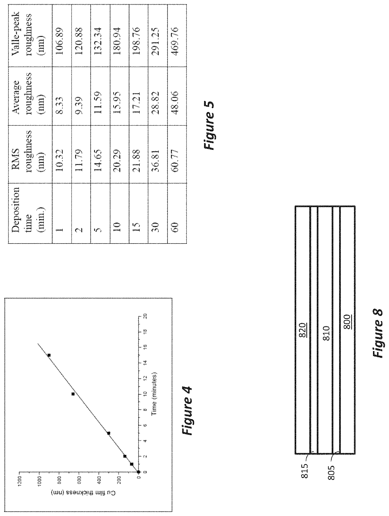
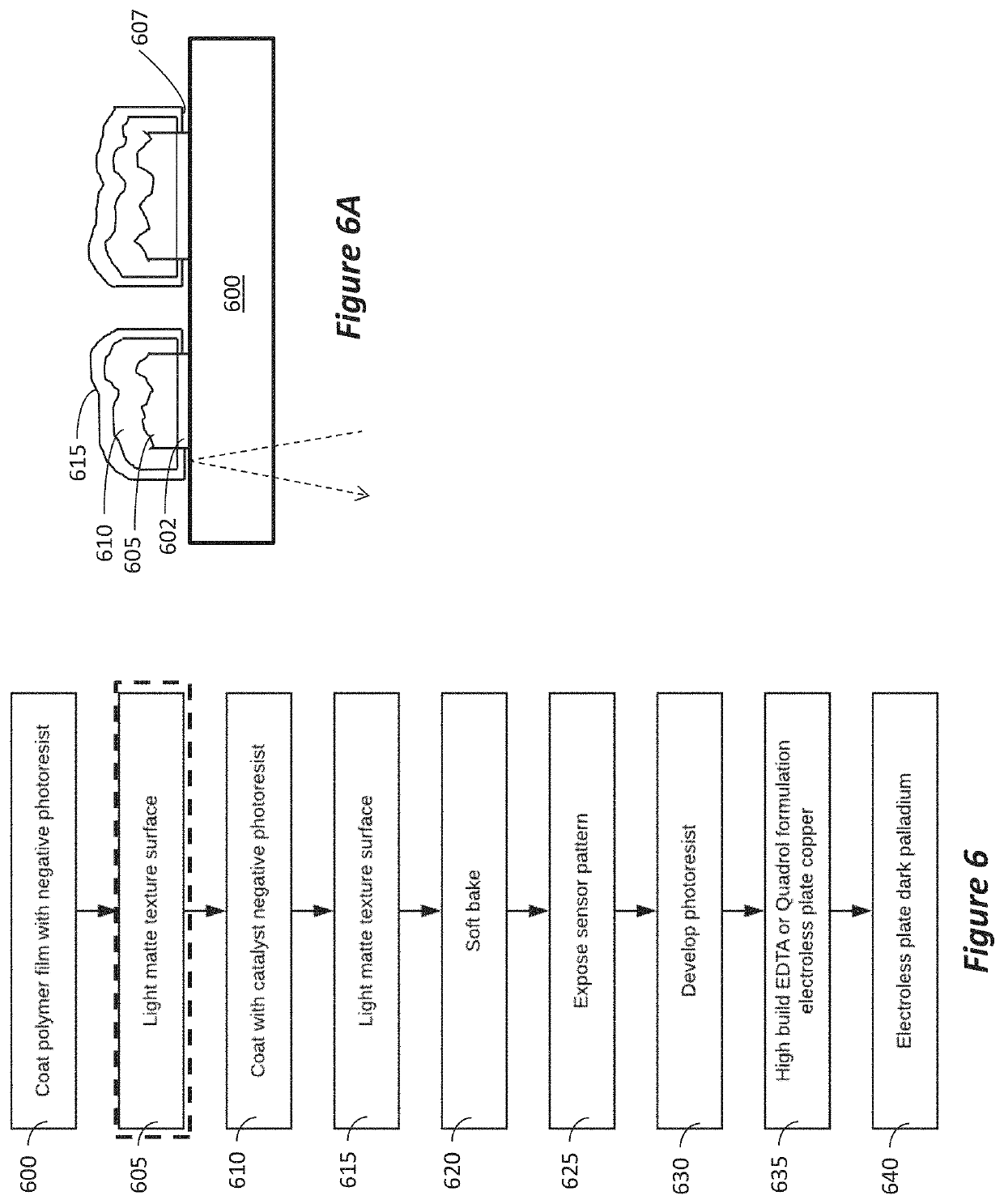
[0033]Disclosed embodiments utilize roughening or nano-texturing in order to scatter incident light to avoid reflection towards the user. The type of surface finish and structure will determine if t...


PUM

PropertyMeasurementUnit
surface roughnessaaaaaaaaaa
RMS surface roughnessaaaaaaaaaa
thicknessaaaaaaaaaa

Abstract

A method for fabricating a metallic wire mesh touch sensor with reduced visibility. A metallic wire mesh is formed on a transparent substrate such that the surface of the metallic wires is roughened or textured, so as to cause high scattering of incident light, thereby minimizing specularly reflected light towards the user. The metal lines are formed over patterned catalytic photoresist. The rough or textured surface of the metallic wires is achieved by roughening or texturing the catalytic photoresist, by selecting parameters of electronless plating of copper, or both. An RMS surface roughness of about 50 nm would scatter approximately 70% of incident cyan light incident at 30°.

Description

BACKGROUND1. Field[0001]This disclosure relates generally to the field of touch sensors. More particularly, the disclosure relates to metallic micro mesh touch sensor for touch screens.2. Related Art[0002]A touch screen enabled system allows a user to control various aspects of the system by finger touch or stylus motion on the screen. A user may interact directly with one or more objects depicted on a display device by fingers or stylus that are sensed by the touch sensor. The touch sensor typically includes a conductive pattern disposed on a substrate configured to sense the exact position of the finger or stylus. Touch screens are commonly used in consumer, commercial, and industrial systems.[0003]The conductive pattern of touch screens has been traditionally made from transparent conductive material, such as indium tin oxide (ITO). However, with the advent of multi-touch screen systems and large displays, it is advantageous to have highly conductive micro mesh systems, for examp...

Claims


Application Information

Patent Timeline
Patent Type & Authority Patents(United States)
IPC IPC(8): G03F7/16C23C18/22C23C18/40C23C18/16G06F3/044B31F1/07
CPCC23C18/22B31F1/07C23C18/165C23C18/405G03F7/16G06F3/044G06F2203/04103G06F2203/04112C23C18/1608C23C18/1612C23C18/1689G06F3/0412G03F7/40G03F7/091G03F7/095G03F7/2022G03F7/0957G03F7/0047G03F7/038C23C18/1603C23C18/1651
Inventor ROUTH, ROBERTMORRIONE, MICHAELHAWTHORNE, JEFFREY
Owner FUTURETECH CAPITAL INC
Why Eureka
Try Eureka