Method of forming nano-patterns on a substrate

a technology of nano-patterns and substrates, applied in the field of forming nano-patterns on substrates, can solve the problems of imposing certain structural limits on the nano-wires for high-resolution colour printing, metals were not allowed in industrial semi-conductor fabrication facilities, and high-resolution colour printing technology, etc., to achieve a surprisingly vivid colour display, reduce the background optical signal, and reduce the effect of ohmic/resistive loss

Active Publication Date: 2022-03-29
AGENCY FOR SCI TECH & RES
View PDF12 Cites 0 Cited by
  • Summary
  • Abstract
  • Description
  • Claims
  • Application Information

AI Technical Summary

Benefits of technology

[0010]Advantageously, the dielectric materials used in the dielectric substrate may have significantly lower Ohmic / resistive loss as compared to the use of noble metals such as gold and silver. More advantageously, the dielectric materials of the present disclosure may be CMOS process compatible. Therefore, the dielectric nanostructures of the present disclosure may be capable of producing high-resolution colour pixels with surprisingly vivid colour display, as compared to the corresponding metallic approach using localized plasmon resonances.
[0011]Advantageously, the addition of an anti-reflectance layer (as shown in the second aspect) may minimize the background optical signal. As a result, the anti-reflectance layer may enhance the colour fidelity significantly in a chromaticity diagram as standardized by the Comission Internationale de l'Eclairage (International Commission on Illumination) (also known as the CIE 1931 chromaticity diagram). More advantageously, the addition of an anti-reflectance layer may achieve superior colour saturation beyond the optical diffraction limit.Definitions

Problems solved by technology

However, there exists one key challenge for the conventional high-resolution colour printing technique relying on plasmonic nanostructures.
As noble metals such as gold could diffuse into silicon, these metals were not allowed in industrial semi-conductor fabrication facilities.
However, such lateral dimensions imposed certain structural limits to the nanowires for high-resolution colour printing beyond the optical diffraction limit.
These absorption peaks, however, were present at a typical full-width-half-maximum (FWHM) of more than 100 nm, which limited the quality of the colours obtained.
Moreover, pitch sizes of 1 μm would limit the number of applications of these long vertical silicon nanowires for achieving colour display that was beyond the diffraction limit.
Furthermore, tall nanostructures were highly difficult to fabricate and maintain.
Therefore, the above dimensions for silicon nanostructures were unsuitable for use.

Method used


Image

  • Method of forming nano-patterns on a substrate
  • Method of forming nano-patterns on a substrate
  • Method of forming nano-patterns on a substrate

Examples


example 1

[0094]Fabrication of Silicon Nanodisks on a Silicon Substrate to Obtain a Basic Colour Palette for High-Resolution Colour Printing

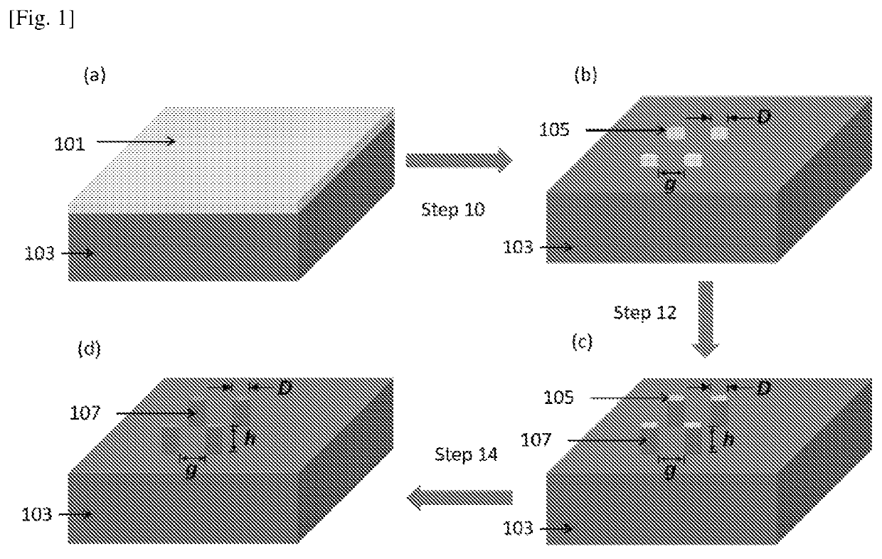
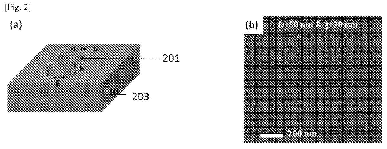
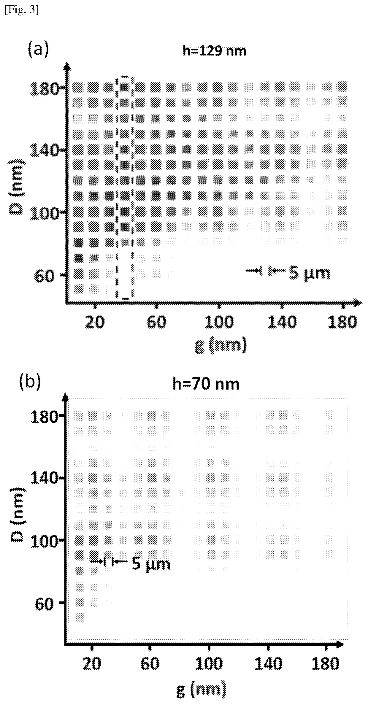
[0095]The method of FIG. 1 is used here to form silicon nanodisks on a silicon substrate. Here, as shown in FIG. 1(a), a resist layer such as hydrogen silsesquioxane (HSQ) (Dow Corning, product number XR-1541-002) was spun coated onto a substrate (103) such as a silicon substrate to form a layer of negative electron-beam resist (101) with a thickness of 30 nm. The HSQ resist was subsequently subjected to electron beam lithography in step 10 to develop the nanodisk mask resists. The HSQ layer was subjected to a negative electron-beam exposure with an electron acceleration voltage of 100 KeV, a beam current of 500 pA and an exposure dosage of 12 mC / cm2. The HSQ resist was then developed by using NaOH / NaCl salt solution (1% wt. / 4% wt. in de-ionized water) for 60 seconds followed by immersion in de-ionized water for another 60 seconds to stop the development....

example 2

[0109]Analysis of Diamond Nanodisks by Scaling Based on a Refractive Index Ratio

[0110]The fabrication method and the analysis of the colour produced of silicon nano disks as described in Example 1 was applied to all other dielectric materials. The corresponding dimensions and inter-structure distances of the nanodisks for all other types of dielectric materials was calculated with reference to the fabricated silicon substrate based on a scaling factor. The scaling factor was defined as the ratio of the refractive index of silicon to the refractive index of a selected dielectric material, i.e., nsi / ndielectric.

[0111]Diamond nanodisks were fabricated from a diamond substrate by simulation using the finite-difference-time-domain (FDTD) method. The corresponding diameter, height and gap size were calculated by multiplying them with the scaling factor. The refractive index of diamond (ndiamond) was 2.4 and the refractive index ratio was calculated to be 1.67. Hence, the scaling factor of...

example 3

[0115]Addition of an Anti-Reflectance Dielectric Layer

[0116]To improve color fidelity of the dielectric nanostructures, an anti-reflectance dielectric layer was inserted between the dielectric nanostructures and dielectric substrate. The anti-reflectance layer significantly enhances the color fidelity of the substrate. The fundamental principle of inserting this anti-reflectance dielectric layer was to minimize the background optical signal, which was not originated from the scattering of the dielectric nano structures.

[0117]In this example, the materials used for both the dielectric nanodisks and dielectric substrates were silicon. The optimal material for the anti-reflectance dielectric layer was determined by a refractive index value calculated based on √{square root over (nairnsub)}, where nair is the refractive index of air and nsub is the refractive index of the base substrate. For a silicon substrate, the optimal anti-reflection dielectric layer should be close to 2.

[0118]The...


PUM

PropertyMeasurementUnit
thicknessaaaaaaaaaa
diameteraaaaaaaaaa
inter-structure distanceaaaaaaaaaa

Abstract

This application relates to a method of forming nano-patterns on a substrate comprising the step of forming a plurality of nanostructures on a dielectric substrate, wherein the nanostructures are dimensioned or spaced apart from each other by a scaling factor of the dielectric substrate with reference to a silicon substrate.

Description

CROSS-REFERENCE TO RELATED APPLICATIONS[0001]This patent application is a U.S. National Phase Application Under 35 U.S.C § 371 of International Application No. PCT / SG2017 / 050440, filed on Sep. 5, 2017, entitled “A METHOD OF FORMING NANO-PATTERNS ON A SUBSTRATE,” which claims the benefit of priority of Singapore Patent Application No. 10201607372X, filed on Sep. 5, 2016.TECHNICAL FIELD[0002]The present invention generally relates to a method of forming nano-patterns on a substrate. The present invention also relates to a nano-patterned substrate formed by the method disclosed herein.BACKGROUND ART[0003]High-resolution colour printing beyond the optical diffraction limit has attracted a great deal of attention in recent years due to its promising applications in the field of Optics. Conventionally, high-resolution colour printing is enabled by the localized plasmon resonance of metallic nanostructures, where each basic colour pixel consisted of metal / HSQ (hydrogen silsesquioxane) nano...

Claims


Application Information

Patent Timeline
Patent Type & Authority Patents(United States)
IPC IPC(8): G02B1/10G02B1/118B82Y40/00B81C1/00G02B1/115G03F7/00H01L21/027H01L21/033H01L21/311
CPCG02B1/118B81C1/00031B81C1/00388B82Y40/00G02B1/115G03F7/0002H01L21/0271H01L21/0337H01L21/31144B81C2201/0149
Inventor YANG, KWANG WEI JOELDONG, ZHAOGANGPANIAGUA-DOMINGUEZ, RAMONKUZNETSOV, ARSENIYYU, YEFENG
Owner AGENCY FOR SCI TECH & RES
Why Eureka
Try Eureka