Voltage-to-time converter architecture for time-domain analog-to-digital converter
- Summary
- Abstract
- Description
- Claims
- Application Information
AI Technical Summary
Benefits of technology
Problems solved by technology
Method used
Image

Examples
Embodiment Construction
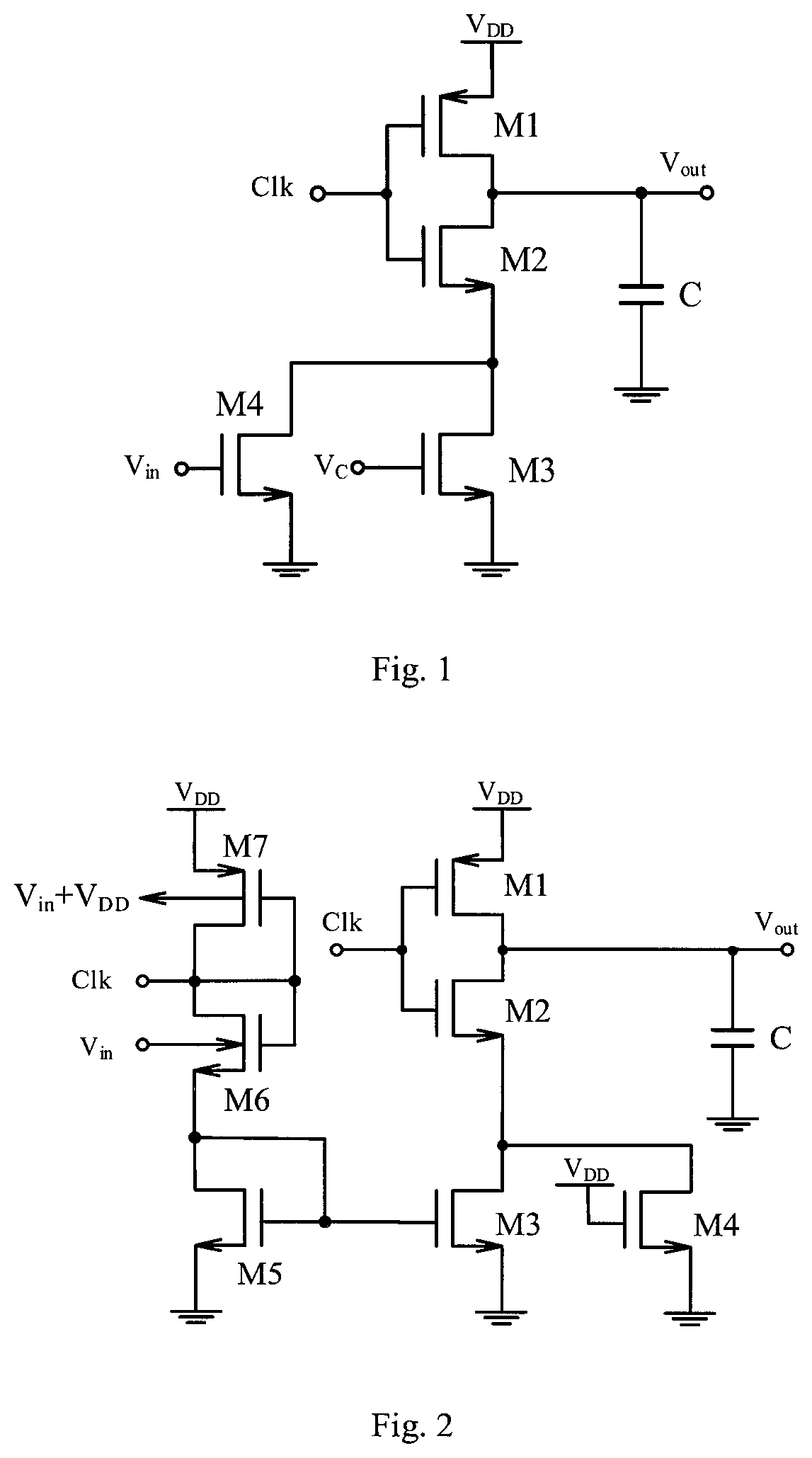
[0018]The invention is characterized in that the input voltage is used as the body terminal or body bias voltage of a PMOS transistor and an NMOS transistor in a current-controlling branch of a current mirror at the same time, thereby generating a high-linearity drain current of an inverter receiving the controlled or mirrored current. The specific working principle of this circuit is as follows.
[0019]Transistors M1 and M2 consist of an inverter. The input terminal of the inverter receives the clock signal Clk. The output terminal outputs the output signal Vout. The transistor M3 is used as a current starving transistor and create a discharge path for the output of inverter circuit to ground. The relationship between the drain current of the branch where M3 is located and the delay time (Td) of the inverter can be simply expressed as:
[0020]Td∝CLIcpVDD
[0021]Where CL is the output load capacitance of the inverter, Icp is the drain current of the inverter branch, and VDD is the supp...
PUM
 Abstract
Description
Claims
Application Information
 - R&D Engineer
- R&D Manager
- IP Professional
- Industry Leading Data Capabilities
- Powerful AI technology
- Patent DNA Extraction
Browse by: Latest US Patents, China's latest patents, Technical Efficacy Thesaurus, Application Domain, Technology Topic.
© 2024 PatSnap. All rights reserved.Legal|Privacy policy|Modern Slavery Act Transparency Statement|Sitemap