Integrated power circuits with distributed bonding and current flow

a power circuit and current flow technology, applied in the field of semiconductor devices, can solve the problems of preventing the implementation of this bond-over-active-circuit concept, affecting the performance of the circuit,

Inactive Publication Date: 2002-01-31
TEXAS INSTR INC
View PDF0 Cites 59 Cited by
  • Summary
  • Abstract
  • Description
  • Claims
  • Application Information

AI Technical Summary

Benefits of technology

0020] Another object of the invention is to provide design and layout concepts and process methods which are flexible so that they can be applied to many families of semiconductor IC products, and are general, so that they can be applied to several generations of products.

Problems solved by technology

Until now, all semiconductor devices manufactured had to exclude the area covered by the bonding pads from use for laying out actual circuit patterns because of the high risk of damaging the circuit structures due to the unavoidable mechanical forces and metallurgical stresses needed in the bonding process.
The cost of applying this polyimide layer has so far prohibited the implementation of this bonds-over-active-circuit concept.
This method requires specific design or redesign of the IC and is poorly suited for standard linear and logic ICs which often have numerous bonding pads but relatively small circuit areas.
It is well known that bonding pads in silicon ICs can be damaged during wafer probing using fine-tip tungsten needles, further during conventional thermosonic wire bonding to aluminum metallization on the circuits, or during solder ball attachment in chip-to-substrate devices of more recent assembly developments.
When the damage is not apparent during the bonding process, the defects may manifest themselves subsequently by succumbing to thermo-mechanical stresses generated during the plastic encapsulation, accelerated reliability testing, temperature cycling, and device operation.
The damage appears in most cases as microcracks which may progress to fatal fractures in the underlying dielectric material, as chip-outs of brittle or mechanically weak dielectric films, often together with pieces of metal or silicon, or as lifted ball bonds, or as delamination of metal layers.
These materials are mechanically weaker than previous standard insulators such as the plasma-enhanced chemical vapor deposited dielectrics.
Since these materials are also used under the bonding pad metal, they magnify the risk of device failure by cracking.
None of these approaches of forming bonds over active circuits exploit the new technical advantages to improve the circuit functions, or propose a method to advance critical device performances.
Together with signal connections, some ICs require more than 1000 contact pads, causing a significant sacrifice of precious silicon "real estate".
Otherwise, the risk of cracking or cratering the layers under the bonding pad has been found to be acceptably high.
Consequently, considerable real estate area of silicon is required just for accommodating the bonding pad.

Method used


Image

  • Integrated power circuits with distributed bonding and current flow
  • Integrated power circuits with distributed bonding and current flow
  • Integrated power circuits with distributed bonding and current flow

Examples


Embodiment Construction

[0063] While this invention has been described in reference to illustrative embodiments, this description is not intended to be construed in a limiting sense. Various modifications and combinations of the illustrative embodiments, as well as other embodiments of the invention, will be apparent to persons skilled in the art upon reference to the description.

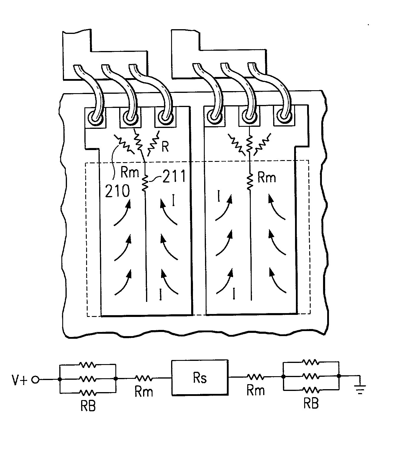
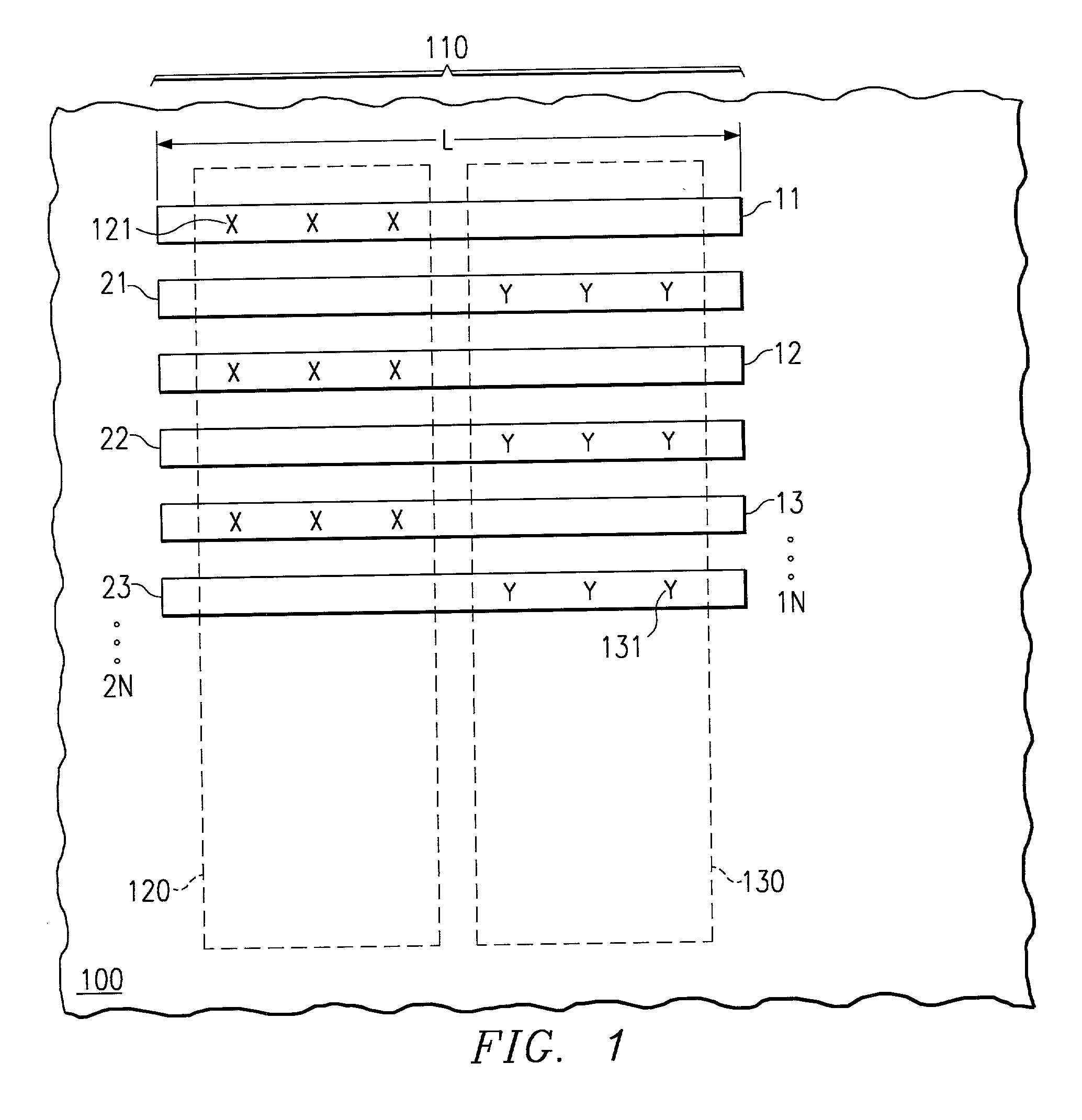
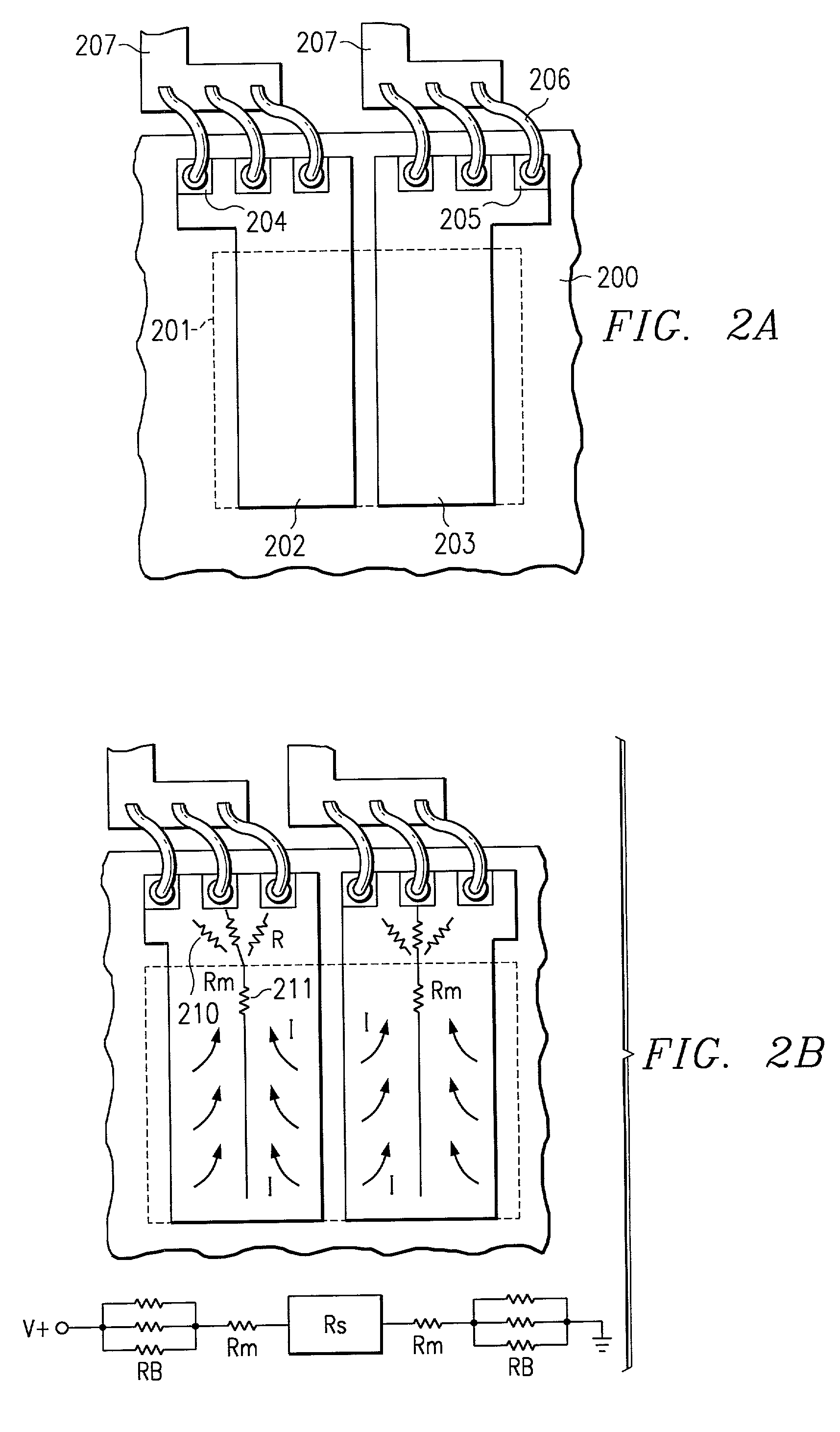
[0064] As an example, the invention covers generally a semiconductor integrated circuit which comprises contact pads located over active components, and the position of these pads are selected so that they provide control and distribution of power to the active components below the pads.

[0065] As another example, the invention covers a semiconductor IC which comprises contact pads located over active components, and these pads are positioned to minimize the distance for power delivery between a selected pad and one or more corresponding active components, to which the power is to be delivered.

[0066] It is therefore intended that t...


PUM


Abstract

A semiconductor integrated circuit comprises contact pads located over active components, which are positioned to minimize the distance for power delivery between a selected pad and one or more corresponding active components, to which the power is to be delivered. This minimum distance further enhances dissipation of thermal energy released by the active components. More specifically, a semiconductor integrated circuit comprises a laterally organized power transistor, an array of power supply contact pads distributed over the transistor, means for providing a distributed, predominantly vertical current flow from the contact pads to the transistor, and means for connecting a power source to each of the contact pads. Positioning the power supply contact pads directly over the active power transistor further saves precious silicon real estate area. The means for vertical current flow include contact pads made of a stack of metal layers comprising refractory metals for adhesion, copper and nickel as stress-absorbing metals, and gold or palladium as bondable and solderable outermost metals. The means for connecting a power source include wire bonding and solder ball interconnection.

Description

[0001] The present invention is related in general to the field of semiconductor devices and processes, and more specifically to integrated power circuits that permit wire bonding to be performed directly over portions of the active circuit area.DESCRIPTION OF THE RELATED ART[0002] Two independent trends in semiconductor technology, both with a long history, contribute to the urgency for the present invention. The first technology trend concerns aspects of manufacturing cost savings by conserving semiconductor "real estate".[0003] In order to accommodate balls of bonding wires or solder, typical bonding pads on silicon integrated circuits (ICs) have to be of sufficient size; they typically range from squares of 80.times.80 .mu.m to squares of 150.times.150 .mu.m. They consume, therefore, an area between approximately 1 and 20%, sometimes up to 45%, of the circuit area, dependent on the number of bonding pads and the size of the integrated circuit. For manufacturing and assembly reas...

Claims


Application Information

Patent Timeline
Patent Type & Authority Applications(United States)
IPC IPC(8): H01L21/3205H01L21/60H01L21/82H01L29/41H01L21/822H01L21/8234H01L23/485H01L23/495H01L23/52H01L23/528H01L27/04H01L27/088H01L29/78
CPCH01L23/4952H01L23/49562H01L23/5286H01L24/03H01L24/05H01L24/06H01L24/45H01L24/48H01L24/49H01L2224/04042H01L2224/05073H01L2224/05082H01L2224/05147H01L2224/05155H01L2224/05157H01L2224/05166H01L2224/05171H01L2224/0518H01L2224/05184H01L2224/05187H01L2224/05624H01L2224/05639H01L2224/05644H01L2224/05655H01L2224/05664H01L2224/05669H01L2224/45015H01L2224/45124H01L2224/45139H01L2224/45144H01L2224/45147H01L2224/45164H01L2224/4554H01L2224/45669H01L2224/48091H01L2224/48227H01L2224/48247H01L2224/4845H01L2224/48465H01L2224/48624H01L2224/48639H01L2224/48644H01L2224/48664H01L2224/48724H01L2224/48739H01L2224/48744H01L2224/48764H01L2224/48824H01L2224/48839H01L2224/48844H01L2224/48864H01L2224/49111H01L2224/49113H01L2224/85205H01L2924/01004H01L2924/01006H01L2924/01013H01L2924/01014H01L2924/01015H01L2924/01022H01L2924/01028H01L2924/01029H01L2924/01031H01L2924/01032H01L2924/01033H01L2924/01039H01L2924/01042H01L2924/01046H01L2924/01047H01L2924/01049H01L2924/0105H01L2924/01074H01L2924/01078H01L2924/01079H01L2924/01082H01L2924/01083H01L2924/01327H01L2924/014H01L2924/04941H01L2924/05042H01L2924/10253H01L2924/14H01L2924/19043H01L2924/20752H01L2924/20753H01L2924/20754H01L2924/30105H01L2924/01019H01L2924/01023H01L2924/01024H01L2924/01037H01L2924/01075H01L2924/01076H01L2224/48755H01L2224/48769H01L2224/48655H01L2224/48669H01L2224/48855H01L2224/48463H01L2224/05553H01L2224/05554H01L2924/00014H01L2924/01007H01L2924/04953H01L2924/00H01L2224/48869H01L2924/20755H01L2924/00015H01L2924/2075
Inventor EFLAND, TAYLOR R.PENDHARKAR, SAMEER
Owner TEXAS INSTR INC
Why Eureka
Try Eureka