Process for polishing silicon wafers

a technology of polishing process and silicon wafer, which is applied in the direction of polishing compositions with abrasives, grinding machines, electrical appliances, etc., can solve the problems of uneven surface of polished silicon surface, inability to deposition epitaxial coatings, and inability to direct further processing of polished silicon surfa

Inactive Publication Date: 2002-05-09
WACKER SILTRONIC
View PDF0 Cites 30 Cited by
  • Summary
  • Abstract
  • Description
  • Claims
  • Application Information

AI Technical Summary

Problems solved by technology

However, incomplete rinsing away of alkaline polishing agent residues may lead to spots being formed on the wafer surface.
There are a number of drawbacks associated with this process.
Firstly, the roughness of the polished silicon surface which is produced does not allow direct further processing.
For example deposition of an epitaxial coating is not allowed or the fabrication of components is not allowed, without following the process with an expensive smoothing touch polishing step.
Thirdly the considerable drop in pH is caused by the addition of the acidic stopping agent, particularly when using large polishing machines which enable 12 or more silicon w

Method used


Image

  • Process for polishing silicon wafers
  • Process for polishing silicon wafers
  • Process for polishing silicon wafers

Examples


invention

EXAMPLE (INVENTION)

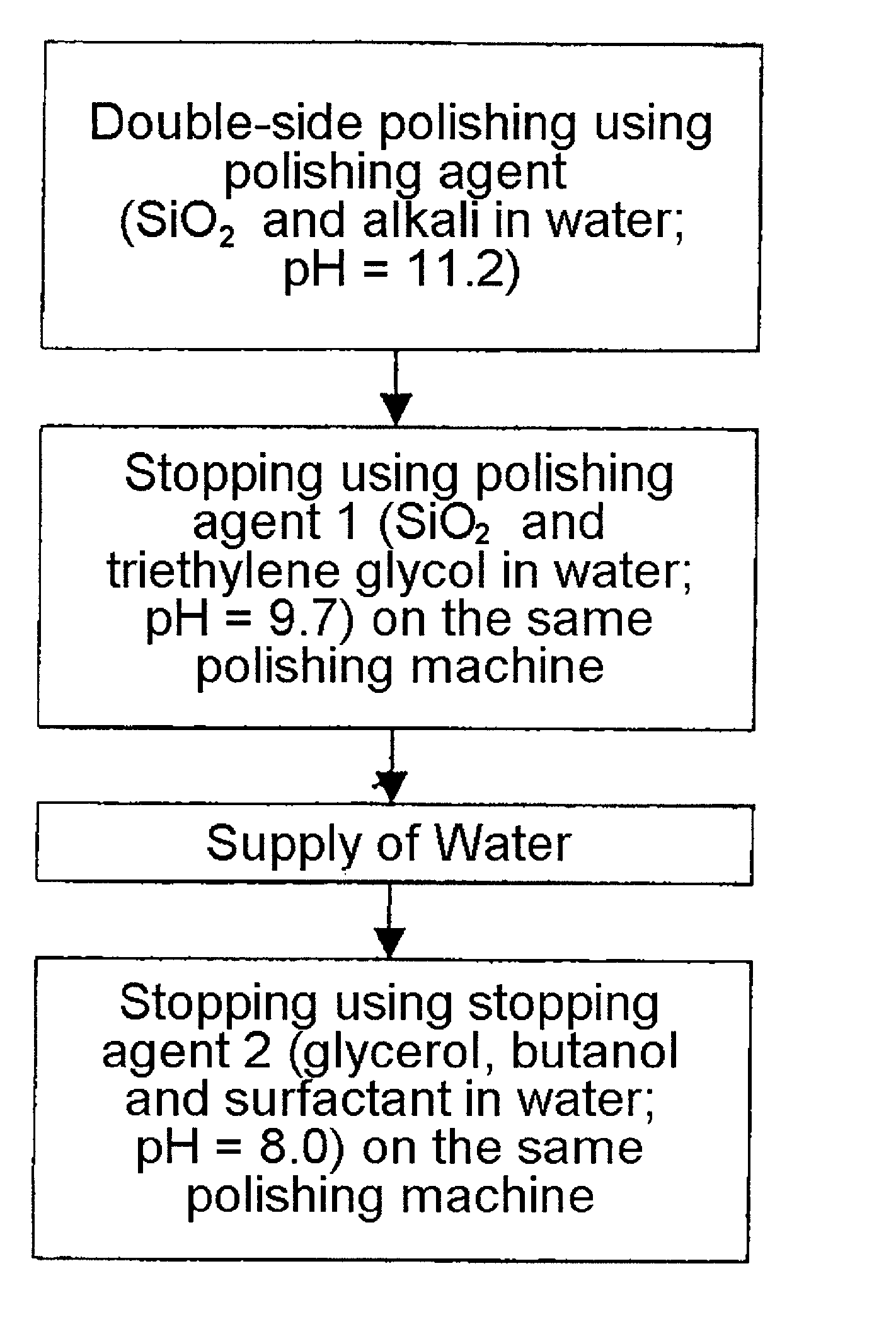
[0039] The procedure was as described in the Comparative Example, except that between the polishing step and the stopping step, with the rotary conditions maintained, a further stopping step followed by a brief feed of ultrapure water, both at a pressure of 0.03 bar, was added. The corresponding stopping agent 1 comprised an aqueous suspension of pyrogenic silica (SiO.sub.2 particle size 30-40 nm; solids content 1.5% by weight; NH.sub.40H-stabilized), to which 0.3% by volume of triethylene glycol was admixed and which had a pH of 9.7. Therefore, to stop the polishing process, the liquids listed below were supplied sequentially: (1) stopping agent 1 (SiO.sub.2 / triethylene glycol in ultrapure water; 3 min); (2) ultrapure water (2 min); (3) stopping agent 2 (glycerol / butanol / surfactant in ultrapure water; 2 min). The silicon wafers produced in this way were likewise substantially free of scratches, haze spots and localized light scatterers.

[0040] Determination of the...


PUM

PropertyMeasurementUnit
Fractionaaaaaaaaaa
Percent by massaaaaaaaaaa

Abstract

A process for the chemical-mechanical polishing of silicon wafers is by rotational movement of the silicon surface which is to be polished on a polishing plate which is covered with polishing cloth, with a continuous supply of an alkaline polishing agent which contains abrasives, at least 2 mum of material being removed from the polished silicon surface during the polishing. Immediately after the polishing has finished, and while maintaining the rotational movement, instead of the polishing agent at least two different stopping agents are supplied in succession, each removing less than 0.5 mum of material from the polished silicon surface.

Description

[0001] 1. Field of the Invention[0002] The present invention relates to a polishing process for semiconductor wafers made from silicon, which are used in particular in industry for the fabrication of microelectronic components.[0003] 2. The Prior Art[0004] Semiconductor wafers made from silicon, which are used as substrates for the fabrication of modern microelectronic components have to fulfill a wide range of properties. These properties are often specified within relatively narrow limits. A number of these quality parameters are only determined in the final processing step of the wafers, generally involving polishing followed by cleaning. Properties of this type include, for example, the planarity of the silicon wafers, their surface roughness and the extent of surface defects, such as scratches, spots and localized light scatterers.[0005] The polishing is generally carried out as a chemical-mechanical process. Here the silicon surface which is to be polished, while an alkaline p...

Claims


Application Information

Patent Timeline
IPC IPC(8): B24B1/00B24B37/04C09G1/02C09K3/14H01L21/302H01L21/304H01L21/306
CPCB24B1/00H01L21/02024C09G1/02B24B37/04H01L21/302
Inventor WENSKI, GUIDOALTMANN, THOMASHEIER, GERHARDWINKLER, WOLFGANG
Owner WACKER SILTRONIC
Why Eureka
Try Eureka