

Plasma processing method and apparatus
a processing method and apparatus technology, applied in the field of plasma processing methods and apparatuses, can solve the problems of charging damage and adverse effect of electron amount on the charge oxide file of the gate oxide fil
- Summary
- Abstract
- Description
- Claims
- Application Information
AI Technical Summary
Benefits of technology
Problems solved by technology
Method used
Image

Examples
first embodiment
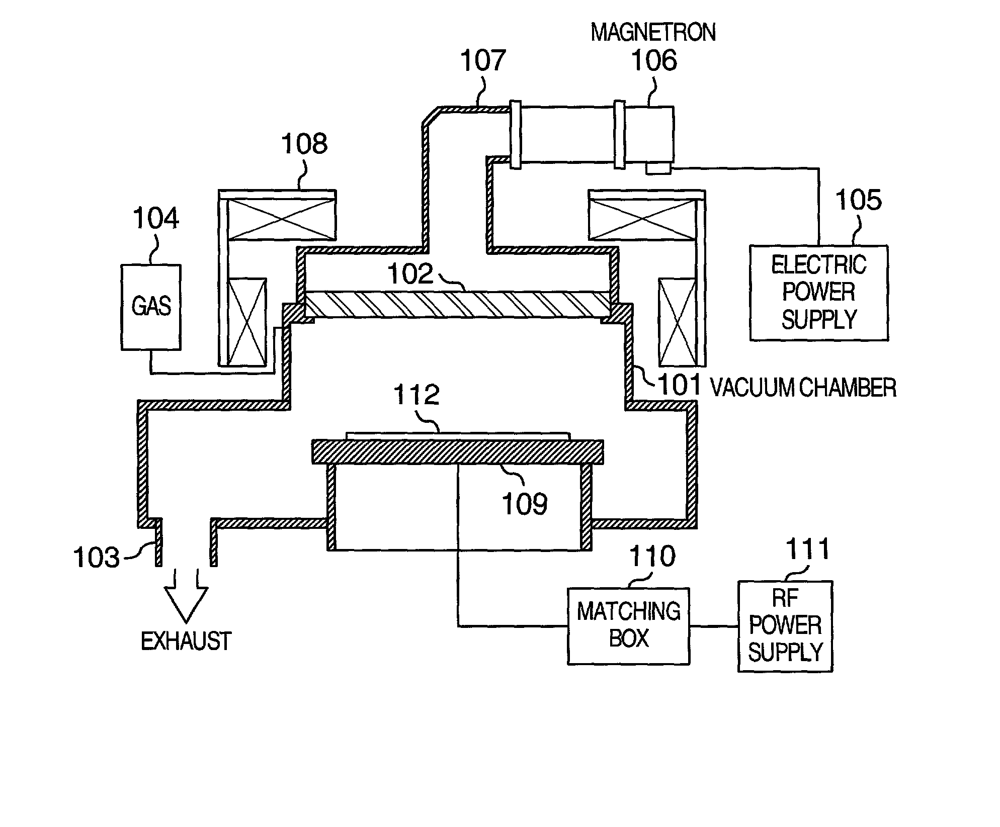
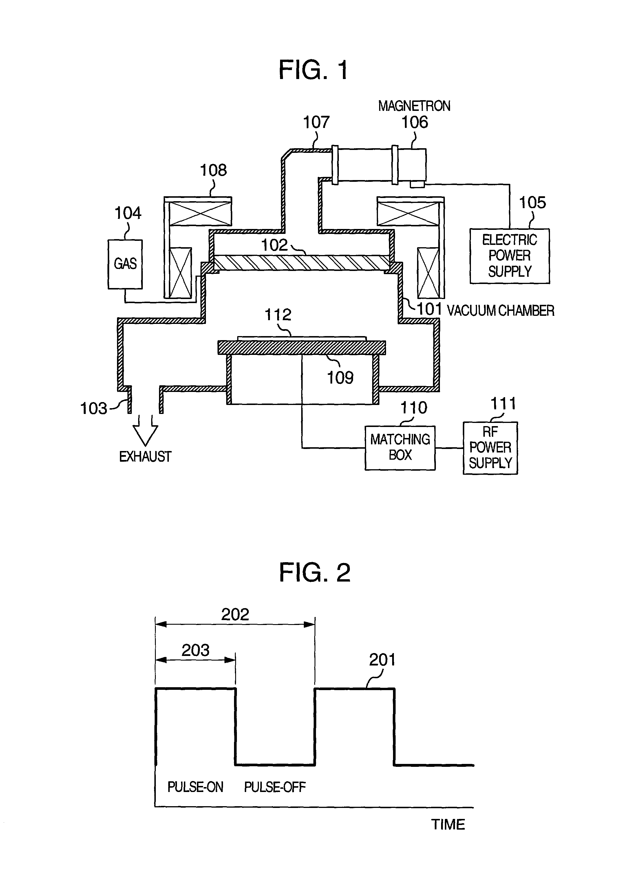
[0035] Hereafter, the present invention will be described with reference to FIGS. 1 to 7. FIG. 1 shows a microwave plasma etching apparatus that is an embodiment of the present invention. A numeral 101 denotes a vacuum chamber the top of which is opened. On the top of the vacuum chamber 101 is placed a dielectric window 102 (such as a quartz window) and then the chamber is sealed. The bottom of the vacuum chamber 101 is connected to a vacuum exhaust device (not shown) through a vacuum exhaust port 103. The upper portion of the vacuum chamber 101 is connected to a gas supply 104. The upper portion of the vacuum chamber 101 is connected to a waveguide 107 and a magnetron 106 through the dielectric window 102. The magnetron 106 is connected to an electric power supply 105 composing a high frequency power supply for generating a plasma together with the magnetron. The electric power supply 105 operates to switch on and off a microwave output at any frequency and any duty ratio. The uppe...
second embodiment
[0053] [Second Embodiment]
[0054] The second embodiment of the present invention will be described with reference to FIG. 8. In this figure, the same numerals as those of FIG. 1 denote the same members about which description will be left out. The different respect of FIG. 8 from that of FIG. 1 will be described below. The upper portion of the vacuum chamber 101 is sealed by a dielectric window 801 (made of quartz, for example) and an upper electrode 802 (made of Si, for example). The upper electrode 802 has a porous structure from which etching gas is flown and is connected to gas supply device 104. The high frequency electric power such as 450 MHz power oscillated by an electric power supply 806 is transmitted to a tuner 804 through a high-pass filter 805. The high frequency electric power such as 13.56 MHz power oscillated by an antenna bias power supply 808 is also transmitted to the tuner 804 through a low-pass filter 807. These high frequency powers are then propagated to the i...
third embodiment
[0055] [Third Embodiment]
[0056] The third embodiment of the present invention will be described with reference to FIG. 9. In FIG. 9, the same numerals as those of FIG. 1 denote the same members. The different respect of FIG. 9 from that of FIG. 1 will be described below. The upper portion of the vacuum chamber 101 is sealed by the dielectric window 801 (made of quartz, for example) and the upper electrode 802 (made of Si, for example). The upper electrode 802 has a porous structure from which the etching gas is to be flown and is connected to the gas supply device 104. A high frequency electric power of, for example, 27 MHz or 60 MHz, oscillated by the electric power supply 903 serving as a high frequency power supply for generating the plasma is propagated to the inside of the vacuum chamber 101 through the upper electrode 802 in which chamber 101 the plasma is generated. The electric power supply 903 may be served to oscillate the modulated pulse. On the other hand, the substrate ...
PUM
| Property | Measurement | Unit |
|---|---|---|
| Fraction | aaaaa | aaaaa |
| Fraction | aaaaa | aaaaa |
| Fraction | aaaaa | aaaaa |
Abstract
Description
Claims
Application Information