Eureka AIR delivers breakthrough ideas for toughest innovation challenges, trusted by R&D personnel around the world.

Mold, method for fabricating mold and pattern formation method

Inactive Publication Date: 2002-09-12
PANASONIC CORP
View PDF8 Cites 42 Cited by
  • Summary
  • Abstract
  • Description
  • Claims
  • Application Information

AI Technical Summary

Benefits of technology

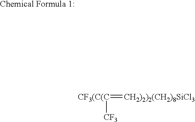
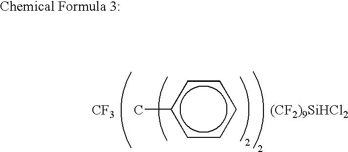
[0026] In the mold of this invention, since n is an integer of 8 or more in the general formula, CF.sub.3(CZ).sub.nSiX.sub.aY.sub.3-a, representing the compound included in the surface treated layer, the molecular chains of monomolecular films of CF.sub.3(CZ).sub.nSi are long, and hence, the interaction between the adjacent molecular chains is so large that the monomolecular films can align without falling down. Therefore, the surface treated layer is covered with CF.sub.3 groups, so that the hydrophobic property of the surface treated layer can be improved and that the resistance of the surface treated layer exhibited in pressing the pressing face of the mold body against the organic film can be improved.
[0055] Thus, the hydrophobic property of the surface treated layer can be further improved, and hence, the organic film pattern is less adhered to the pressing face in moving the mold away from the organic film pattern.

Problems solved by technology

Although a conventional resist pattern is formed by the lithography, it has become very difficult to form a fine resist pattern of 100 nm or less by the lithography because of, for example, a limit on reducing the wavelength of exposing light.
Also, the lithography using EB (electron beams) as the exposing light has a merit in the resolution but is difficult to apply to the mass production because of low throughput.
When the shape of the organic film pattern 4A is defective, an interconnect pattern formed by using the organic film pattern 4A as a mask is also in a defective shape, resulting in disadvantageously lowering the yield of semiconductor devices.
Accordingly, the shape of an interconnect pattern formed by using the organic film pattern 4B as a mask cannot be satisfactory, and hence, the yield of semiconductor devices cannot be sufficiently improved.

Method used


Image

  • Mold, method for fabricating mold and pattern formation method
  • Mold, method for fabricating mold and pattern formation method
  • Mold, method for fabricating mold and pattern formation method

Examples


embodiment 1

[0068] Embodiment 1

[0069] Embodiment 1 of the invention will now be described with reference to FIGS. 1A through 1C and 2A through 2C.

[0070] First, as shown in FIG. 1A, a reverse pattern 11 corresponding to a mirror image of a pattern to be transferred (for example, an interconnect pattern), which is obtained by reversing the pattern to be transferred, is formed from a silicon oxide film on a mold substrate 10. Thus, a mold body composed of the mold substrate 10 and the reverse pattern 11 can be obtained. The reverse pattern 11 may be formed from a silicon film or a silicon carbide film instead of the silicon oxide film.

[0071] Next, the mold is immersed in a 0.2 wt % CF.sub.3(CF.sub.2).sub.7(C- H.sub.2).sub.2SiCl.sub.3 solution (solvent: a mixture of hexadecane and chloroform in a weight ratio of 4:1) for 10 minutes in a dry atmosphere (including substantially no moisture), such as an atmosphere with a water vapor concentration of 0.006 kg / m.sup.3. Thus, a surface treated layer 12 i...

embodiment 2

[0078] Embodiment 2

[0079] Embodiment 2 of the invention will now be described with reference to FIGS. 3A through 3D.

[0080] First, as shown in FIG. 3A, a reverse pattern 21 corresponding to a mirror image of a pattern to be transferred (for example, a contact hole), which is obtained by reversing the pattern to be transferred, is formed from a silicon oxide film on a mold substrate 20. Thus, a mold body composed of the mold substrate 20 and the reverse pattern 21 is obtained. The reverse pattern 21 may be formed from a silicon film or a silicon carbide film instead of the silicon oxide film.

[0081] Next, the mold body composed of the mold substrate 20 and the reverse pattern 21 is immersed in a 0.3 wt % CF.sub.3(CH.sub.2).sub.9Si(C- H.sub.3)Cl.sub.2 solution (solvent: a mixture of hexadecane and chloroform in a weight ratio of 4:1) for 10 minutes in a dry atmosphere (including substantially no moisture), such as an atmosphere with a water vapor concentration of 0.005 kg / m.sup.3. Thus,...

embodiment 3

[0085] Embodiment 3

[0086] Embodiment 3 of the invention will now be described with reference to FIGS. 4A through 4D and 5A through 5C.

[0087] First, as shown in FIG. 4A, a reverse pattern 31 corresponding to a mirror image of a pattern to be transferred (for example, an interconnect groove), which is obtained by reversing the pattern to be transferred, is formed from a silicon oxide film on a mold substrate 30. Thus, a mold body composed of the mold substrate 30 and the reverse pattern 31 is obtained. The reverse pattern 31 may be formed from a silicon film or a silicon carbide film instead of the silicon oxide film.

[0088] Next, the mold body composed of the mold substrate 30 and the reverse pattern 31 is immersed in a 0.2 wt % CF.sub.3(CF.sub.2).sub.8SiCl- .sub.3 solution (solvent: a mixture of hexadecane and chloroform in a weight ratio of 4:1) for 5 minutes in a dry atmosphere (including substantially no moisture), such as an atmosphere with a water vapor concentration of 0.006 kg...


PUM

PropertyMeasurementUnit
Weight per unit lengthaaaaaaaaaa
Concentrationaaaaaaaaaa

Abstract

A mold body included in a mold of the invention has a pressing face. A surface treated layer including a compound represented by a general formula, CF.sub.3(CZ).sub.nSiX.sub.aY.sub.3-a, wherein n is an integer of 8 or more; a is 1, 2 or 3; Z are the same or different and selected from the group consisting of a hydrogen atom, a halogen atom, a substituted or non-substituted saturated or unsaturated alkyl group and a substituted or non-substituted aromatic group; X is a halogen atom; and Y is a hydrogen atom or a saturated alkyl group, is formed at least on the pressing face of the mold body.

Description

BACKGROUND OF THE INVENTION[0001] The present invention relates to a mold for use in an imprint method, a method for fabricating the mold and a pattern formation method using the mold.[0002] In accordance with improvement in the degree of integration of semiconductor integrated circuits, there are increasing demands for refinement of a resist pattern formed by lithography.[0003] Although a conventional resist pattern is formed by the lithography, it has become very difficult to form a fine resist pattern of 100 nm or less by the lithography because of, for example, a limit on reducing the wavelength of exposing light.[0004] Also, the lithography using EB (electron beams) as the exposing light has a merit in the resolution but is difficult to apply to the mass production because of low throughput.[0005] Therefore, a method for forming a fine pattern with high productivity by using an imprint method has been proposed (for example, S. Y. Chou et al., Appl. Phys. Lett., vol. 67, p. 3114...

Claims


Application Information

Patent Timeline
IPC IPC(8): H01L21/30B29C33/42B29C33/56B29C33/60B29C59/00G03F7/00H01L21/027
CPCB29C33/424B29C33/56B29C33/60B29C59/00B82Y10/00B82Y40/00G03F7/0002
Inventor ENDO, MASAYUKISASAGO, MASARUMINO, NORIHISAOGAWA, KAZUFUMIHIRAI, YOSHIHIKO
Owner PANASONIC CORP
Why Eureka
Eureka Blog
Learn More