Conditioner and conditioning disk for a CMP pad, and method of fabricating, reworking, and cleaning conditioning disk

a technology of conditioning disk and cmp pad, which is applied in the direction of grinding device, abrasive surface conditioning device, cleaning using liquids, etc., can solve the problems of many process failures in the semiconductor device fabrication process, complex surface structure of these semiconductor devices, and many step height differences between intermediary layers. to achieve the effect of efficient conditioning the polishing pad

Inactive Publication Date: 2002-09-12
SAMSUNG ELECTRONICS CO LTD
View PDF0 Cites 65 Cited by
  • Summary
  • Abstract
  • Description
  • Claims
  • Application Information

AI Technical Summary

Benefits of technology

0018] The present invention is directed to providing a conditioning disk for a chemical mechanical polishing (CMP) pad for efficiently conditioning the polishing pad, and a method of fabricating the conditioning disk.

Problems solved by technology

This means that the surface structure of these semiconductor devices is more complicated, and step height differences between intermediary layers are more severe.
These step height differences cause many process failures in the semiconductor device fabrication process, for example, in the photolithography process for forming a photoresist pattern on a semiconductor wafer, which comprises the steps of coating the wafer with photoresist, aligning a mask having circuit patterns with the wafer having photoresist thereon, and performing an exposure process and a development process.
However, the step height difference is increasing due to the finer patterns and multilayered structure of the modern devices.
Therefore, it is more difficult to focus between the upper and the lower position of the step height during the exposure process, and it is also difficult to obtain more precise patterns.
A planarization technique such as SOG (Spin On Glass) film deposition has been introduced, or a partial planarization technique, such as etch back or reflow, etc., has been used, but many problems persist.
Therefore, the surface of the polishing pad 12 becomes slippery with repeated CMP processing, thereby abruptly decreasing the removal rate for subsequent wafers.
As a result, the conditioning disk 24 has a short life time, and frequent replacement of the conditioning disk 24 results in decreased productivity and deterioration of production yield due to increased process failures.

Method used


Image

  • Conditioner and conditioning disk for a CMP pad, and method of fabricating, reworking, and cleaning conditioning disk
  • Conditioner and conditioning disk for a CMP pad, and method of fabricating, reworking, and cleaning conditioning disk
  • Conditioner and conditioning disk for a CMP pad, and method of fabricating, reworking, and cleaning conditioning disk

Examples


Embodiment Construction

[0049] Reference will now be made in detail to preferred embodiments of the present invention, examples of which are illustrated in the accompanying drawings.

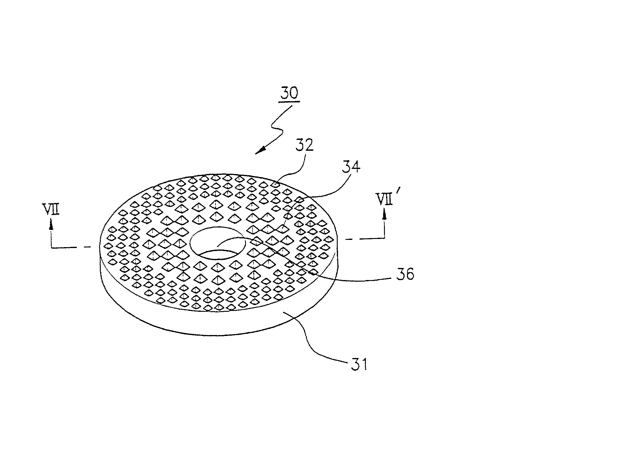
[0050] A conditioning disk for conditioning the surface of a polishing pad during the CMP (chemical mechanical polishing) process according to the present invention is described in detail.

[0051] The conditioning disk is made of metallic material, and its diameter is 90 to 110 mm. Abrasive grains, e.g. artificial diamonds, are provided on the surface of the conditioning disk protruding from its surface, wherein the artificial diamonds form specific distribution regions.

[0052] The artificial diamonds are distributed radially, forming a plurality of concentric ringed-regions, and preferably, the different regions being defined by the size of the artificial diamonds therein. For example, one region may contain artificial diamonds greater than 200 .mu.m in size, and a second region may contain artificial diamonds having a size less ...


PUM

PropertyMeasurementUnit
diameteraaaaaaaaaa
sizeaaaaaaaaaa
sizeaaaaaaaaaa

Abstract

A conditioning disk and a conditioner for a chemical mechanical polishing (CMP) pad, and a method of fabricating, reworking, and cleaning the conditioning disk, are utilized to improve conditioning efficiency, and to reduce production expenses. The conditioning disk for a CMP pad is divided into regions defined by a size difference of abrasive grains formed on the body surface in each region of the conditioning disk. The method of fabricating the conditioning disk is performed by forming adhesive films for attaching the abrasive grains onto the body surface multiple times. In addition, a used conditioning disk may be reworked by detaching the abrasive grains from the body, and attaching new abrasive grains. A used conditioning disk can also be cleaned of by-products of the conditioning process by a cleaning method using a HF solution or BOE (buffered oxide etch) solution.

Description

BACKGROUND OF THE INVENTION[0001] 1. Field of the Invention[0002] The present invention relates to chemical mechanical polishing (CMP), and more particularly, to a conditioner and a conditioning disk for conditioning a CMP pad, and a method of fabricating, reworking, and cleaning the conditioning disk.[0003] 2. Background of the Related Art[0004] Highly integrated semiconductor devices require a sophisticated pattern formation technique, and use a multilayer structure for circuit distribution. This means that the surface structure of these semiconductor devices is more complicated, and step height differences between intermediary layers are more severe.[0005] These step height differences cause many process failures in the semiconductor device fabrication process, for example, in the photolithography process for forming a photoresist pattern on a semiconductor wafer, which comprises the steps of coating the wafer with photoresist, aligning a mask having circuit patterns with the waf...

Claims


Application Information

Patent Timeline
Patent Type & Authority Applications(United States)
IPC IPC(8): B24B53/017B24B53/14B24B53/12B24D3/00B24D3/06B24D7/00B24D7/06B24D7/14B24D18/00H01L21/304
CPCB24B53/017B24B53/12B24D3/06B24D7/06B24D18/0072Y10S438/959H01L21/304
Inventor CHO, SUNG-BUMCHOI, BAIK-SOONKIM, JIN-SUNGCHOI, KYUE-SANG
Owner SAMSUNG ELECTRONICS CO LTD
Why Eureka
Try Eureka