
Method and apparatus for avoiding particle accumulation in electrodeposition

a particle and electrodeposition technology, applied in the direction of lapping machines, manufacturing tools, abrasive surface conditioning devices, etc., can solve the problems of increasing in size, increasing in size, and increasing in cost and time, and achieve the effect of reducing the defect of the workpi

Inactive Publication Date: 2002-10-03
NOVELLUS SYSTEMS
View PDF0 Cites 12 Cited by
  • Summary
  • Abstract
  • Description
  • Claims
  • Application Information

AI Technical Summary

Benefits of technology

[0015] It is yet another object of the invention to reduce defects on the workpiece.

Problems solved by technology

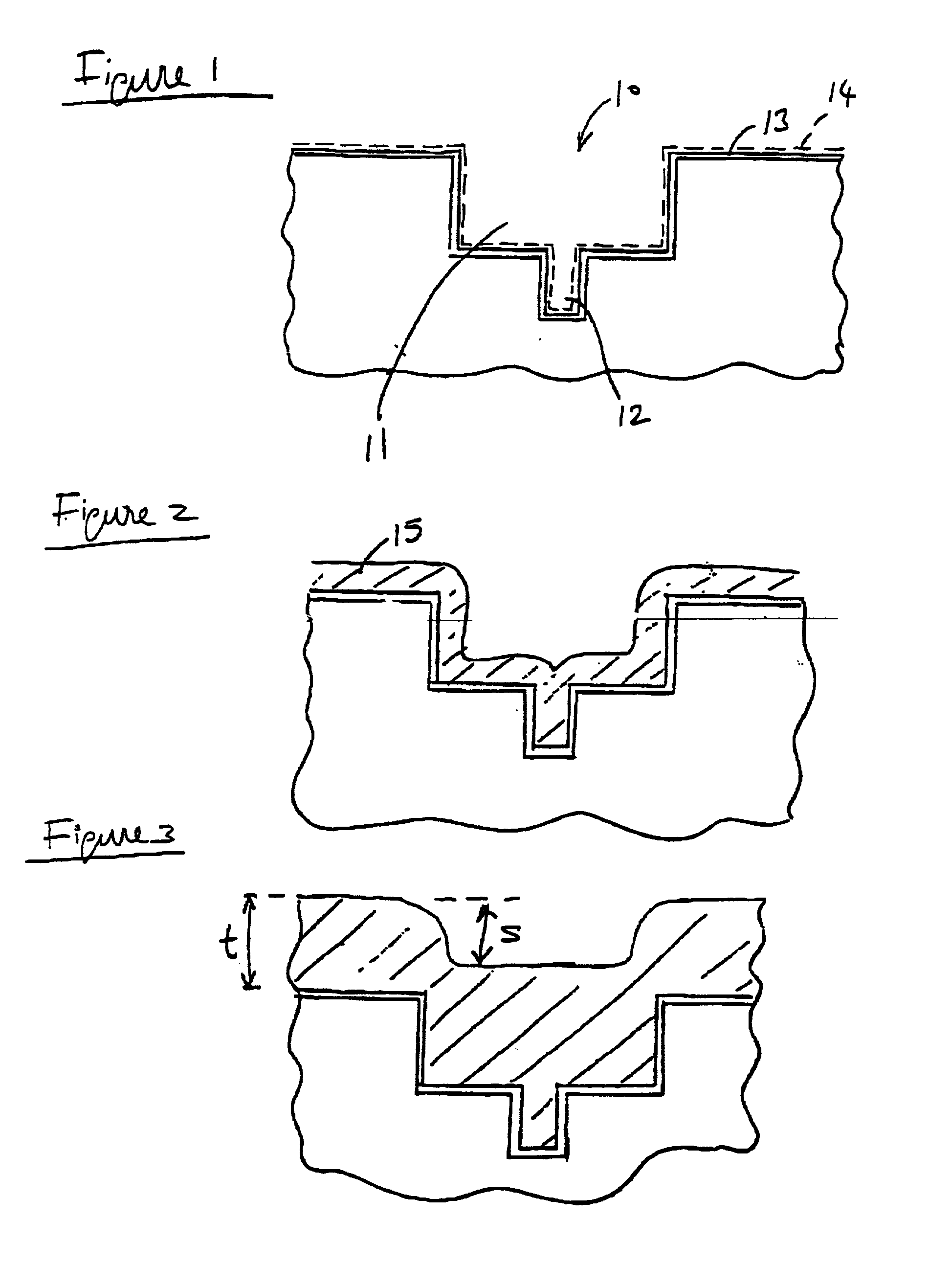
Thick copper on the surface presents a problem during the material removal step such as a CMP step, which is expensive and time consuming.
These particles may exist because of the fact that they may be just physically removed from the substrate surface or they may originate from the plating solution due to poor filtration of the plating solution.
In any case once the conductive metal particles attach themselves to a location on the WSID, they may start growing in size because they become cathodic with respect to the electrode.
Further, since they are conductive they receive coating and thus grow in size.
The non-conductive particles may originate from other parts of the system, such as from the plating solution due to the poor filtration or from the WSID material itself due to the wear and tear during processing.
Presence of such particles on or in close proximity of the surface of the WSID is undesirable because if they become loose and find their way to the interface between the WSID and the workpiece surface, they can cause scratches, inclusions, or other defects on the workpiece surface or they can actually cause scratches on the surface of the WSID, especially if the WSID has a non-flat surface profile.

Method used


Image

  • Method and apparatus for avoiding particle accumulation in electrodeposition
  • Method and apparatus for avoiding particle accumulation in electrodeposition
  • Method and apparatus for avoiding particle accumulation in electrodeposition

Examples


Embodiment Construction

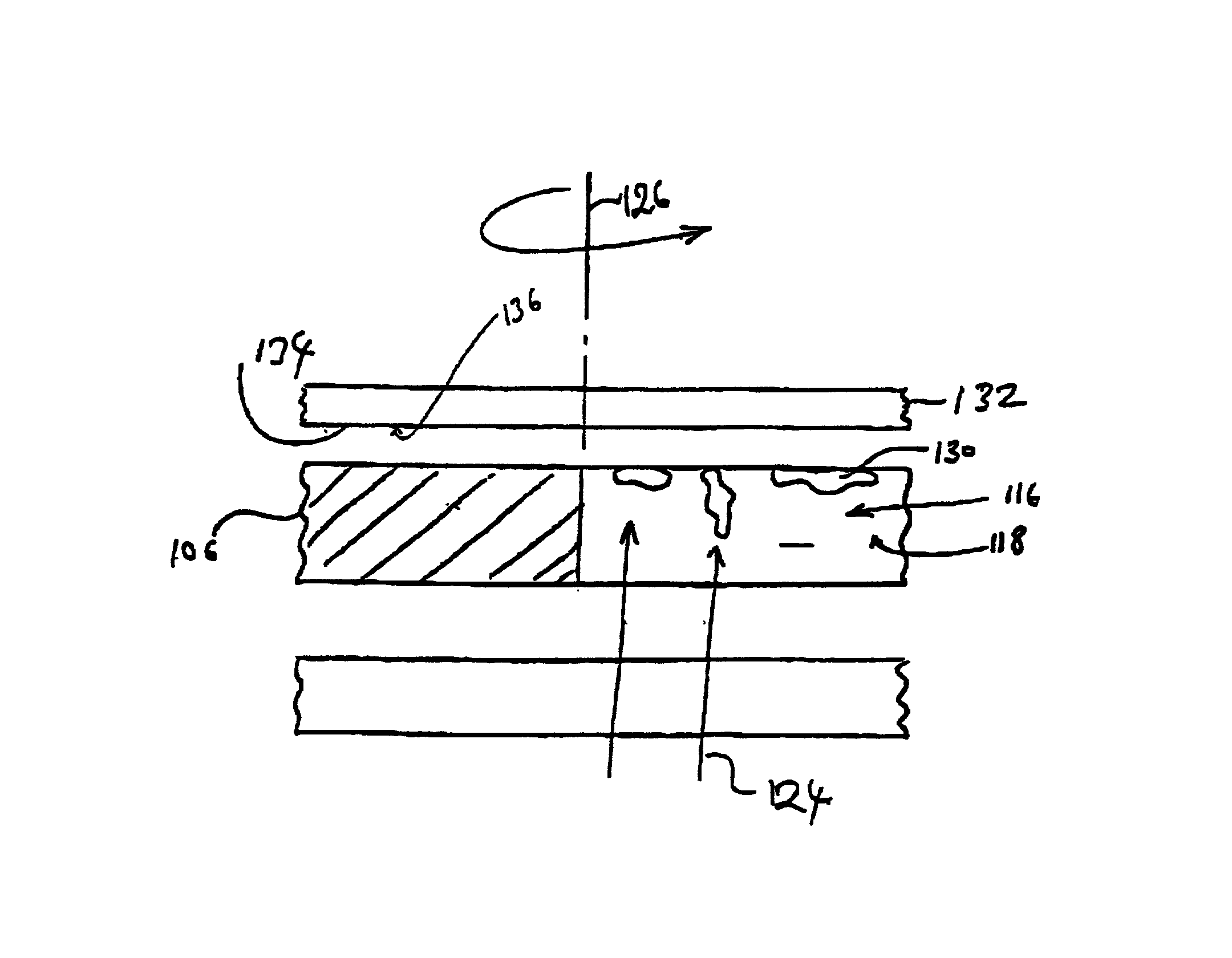
[0039] One way of eliminating the growth of conductive, and typically metallic, or other particles on the workpiece surface influencing device (WSID) surface is to use a "particle elimination step" during electrochemical mechanical processing, either simultaneous with the electrochemical mechanical processing or when intermittently stopping the electrochemical mechanical processing. This step involves using a conditioning system, with a conditioning member that can assist in removing particles. As described hereinafter, this conditioning member can take the form of a conditioning substrate with a plurality of brushes that operates mechanically, a conductive conditioning substrate with conductive brushes that operates both mechanically and electrically, or a conditioning conductor layer that operates electrically. Of course, modifications of these embodiments can also exist. When operating electrically, as described hereinafter, the conductor used to coat is preferably an inert mater...


PUM

PropertyMeasurementUnit
Timeaaaaaaaaaa
Polarityaaaaaaaaaa
Sizeaaaaaaaaaa

Abstract

Systems and methods to remove or lessen the size of metal particles that have formed on, and to limit the rate at which metal particles form or grow on, workpiece surface influencing devices used during electrodeposition are presented. According to an exemplary method, the workpiece surface influencing device is occasionally placed in contact with a conditioning substrate coated with an inert material, and the bias applied to the electrodeposition system is reversed. According to another exemplary method, the workpiece surface influencing device is conditioned using mechanical contact members, such as brushes, and conditioning of the workpiece surface influencing device occurs, for example, through physical brushing of the workpiece surface influencing device with the brushes. According to a further exemplary method, the workpiece surface influencing device is rotated in different direction during electrodeposition.

Description

[0001] 1. Field of the Invention[0002] The present invention relates to a method and apparatus for removing particles from surfaces, and avoiding particle accumulation on surfaces during, electrochemical mechanical processing.[0003] 2. Description of the Related Art[0004] Conventional semiconductor devices generally include a semiconductor substrate, usually a silicon substrate, and a plurality of sequentially formed dielectric interlayers such as silicon dioxide and conductive paths or interconnects made of conductive materials. The interconnects are usually formed by filling a conductive material in trenches etched into the dielectric interlayers. In an integrated circuit, multiple levels of interconnect networks laterally extend with respect to the substrate surface. The interconnects formed in different layers can be electrically connected using vias or contacts. A conductive material filling process of such features, i.e., via openings, trenches, pads or contacts can be carried...

Claims


Application Information

Patent Timeline
IPC IPC(8): B08B1/04B24B37/04B24B53/00B24B53/007C25D5/22C25D7/12C25F3/16H01L21/288H01L21/304H01L21/768
CPCB24B37/04B24B53/001B24B53/017C25D17/001H01L21/2885H01L21/7684H01L21/76877C25D5/22H01L21/306
Inventor BASOL, BULENT M.UZOH, CYPRIANTALIEH, HOMAYOUN
Owner NOVELLUS SYSTEMS
Learn More