Method and device for controlling liquid flow on the surface of a microfluidic chip

a microfluidic chip and liquid flow technology, applied in mechanical equipment, transportation and packaging, laboratory glassware, etc., can solve the problems of micromechanical devices with limitations, moving parts such as miniature pumps and gears, often suffering leakage and degradation under wear, electrokinetic and pneumatic techniques

Inactive Publication Date: 2002-10-17
CALIFORNIA INST OF TECH
View PDF7 Cites 135 Cited by
  • Summary
  • Abstract
  • Description
  • Claims
  • Application Information

AI Technical Summary

Problems solved by technology

Micromechanical devices have the limitation that moving parts, such as miniature pumps and gears, often suffer leakage and degradation under wear.
Electrokinetic and pneumatic techniques have the limitation that because the flow is confined to interior channels, particulates and aggregates in solution can block flow and destroy pumping action.
Each of the above-described devices also has the limitation of being capable of handling either continuous streams or discrete droplets but not both due to the flow mechanism on which they are based.
The mixing of liquids in microscale devices is often difficult to attain due to the absence of turbulent phenomena.
Glycerol does not adhere to hydrophobic coatings and does not readily evaporate at room temperature.

Method used


Image

  • Method and device for controlling liquid flow on the surface of a microfluidic chip
  • Method and device for controlling liquid flow on the surface of a microfluidic chip
  • Method and device for controlling liquid flow on the surface of a microfluidic chip

Examples


example i

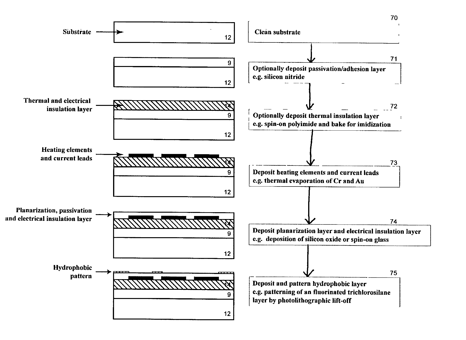
[0078] Prototypes for the sensor device depicted in FIGS. 11a and 11b have been fabricated using the following process steps:

[0079] 1. Cutting of silicon wafers into 2-by-2 inch pieces.

[0080] 2. Cleaning of silicon samples by rinsing with or ultrasonication in tetrachlorethylene, acetone and isopropanol.

[0081] 3. Further cleaning of silicon samples by immersion into a mixture of sulfuric acid, hydrogen peroxide and deionized water at a temperature of 80.degree. C. for 20 minutes.

[0082] 4. Deposition of a 120 nm thick layer of silicon dioxide by plasma enhanced chemical vapor deposition using a Plasmatherm 790 at a temperature of 250.degree. C.

[0083] 5. Deposition of a 120 nm thick layer of silicon nitride by plasma enhanced chemical vapor deposition using a Plasmatherm 790 at a temperature of 250.degree. C.

[0084] 6. Deposition of a 120 nm thick layer of silicon dioxide by plasma enhanced chemical vapor deposition using a Plasmatherm 790 at a temperature of 250.degree. C.

[0085] 7. Sp...

example ii

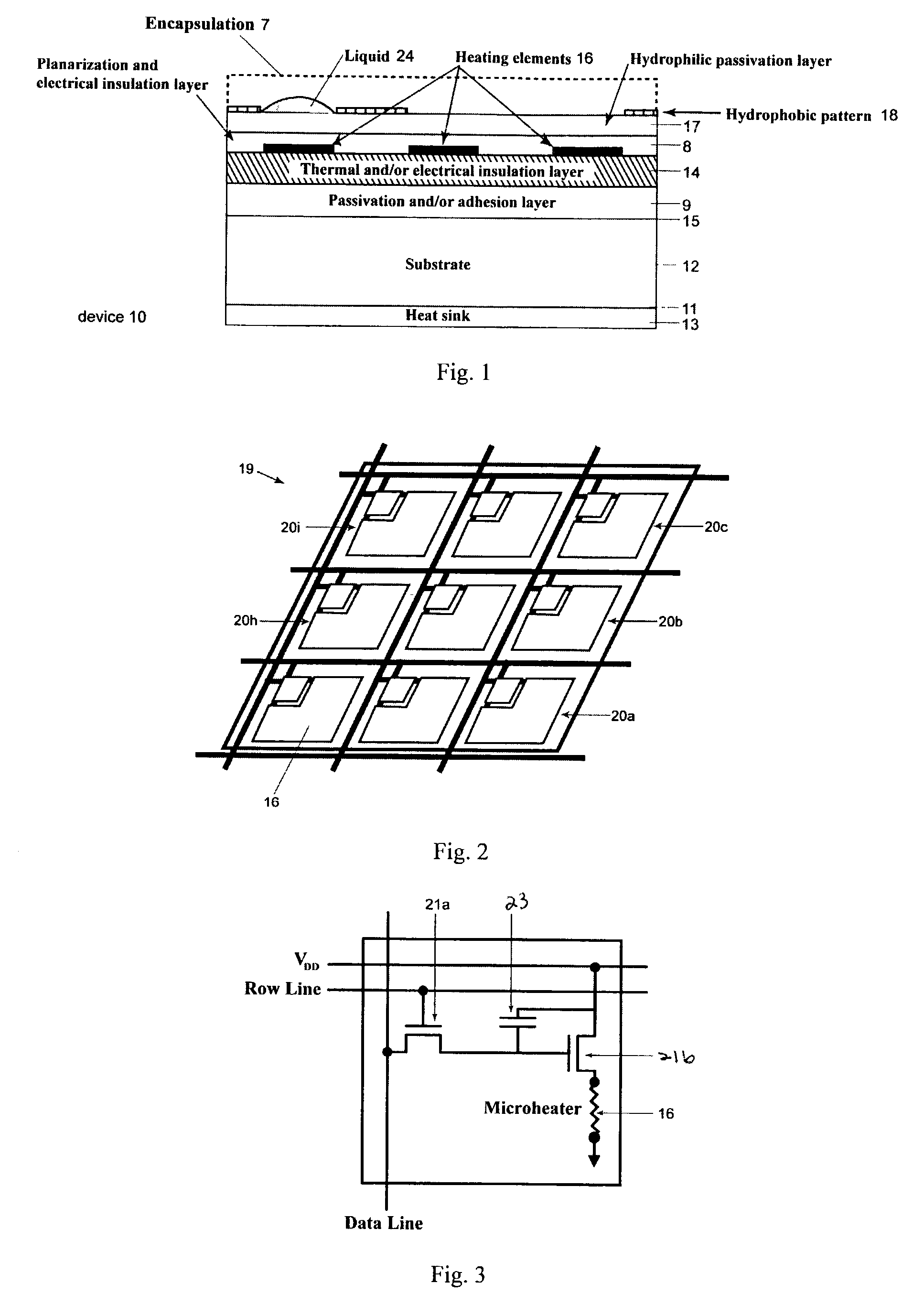
[0102] Another prototype for the sensor device depicted in FIG. 1b and 1c has been fabricated using the following process steps:

[0103] 1. Cutting of silicon wafers in 2-by-2 inch pieces

[0104] 2. Cleaning of silicon samples by rinsing with or ultrasonication in tetrachlorethylene, acetone and isopropanol

[0105] 3. Further cleaning of silicon samples by immersion into a mixture of sulfuric acid, hydrogen peroxide and deionized water at a temperature of 80.degree. C. for 20 minutes.

[0106] 4. Spin-coating of a layer of photoresist (AZ5214 at 4000 rpm for 40 seconds), exposure to UV radiation in a Karl Suess MJB3 mask aligner with a photolithographic mask for straight parallel hydrophilic channels and development of the photoresist using Clariant 400k developer

[0107] 5. Immersion of sample in a dilute (1 mM) solution of 1H,1H,2H,2H-perfluorooctyttrichlorosilane in dodecane for 5 ml.

[0108] 6. Removal of sample from solution and sonication of sample in dodecane for 1-5 minutes.

[0109] 7. Sam...

example iii

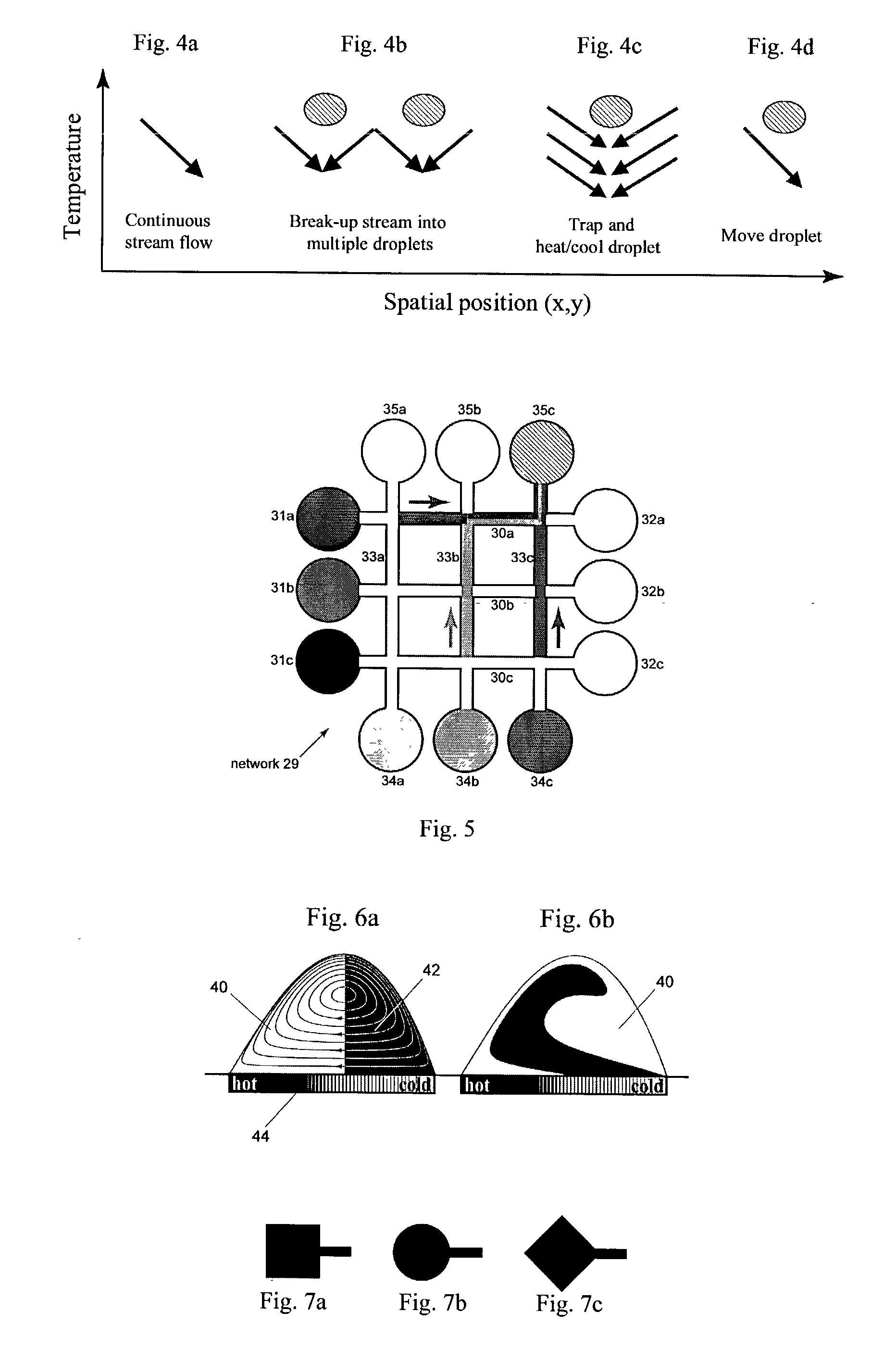
[0119] A prototypes for the microfluidic routing device depicted in FIG. 1a has been fabricated using the following process steps:

[0120] 1. Cleaning of a 2-by-2 inch piece of Corning 1737 glass with a thickness of 0.7 mm by rinsing with (or ultrasonication in) tetrachlorethylene, acetone and isopropanol.

[0121] 2. Further cleaning by immersion into a mixture of sulfuric acid, hydrogen peroxide and deionized water at a temperature of 80.degree. C. for 20 minutes.

[0122] 3. Spin coating of a layer of photoresist (AZ5214 at 4000 rpm for 40 seconds), exposure to UV radiation in a Karl Suess MJB3 mask aligner with a photolithographic mask for the heating electrodes and development of photoresist using Clariant 400k developer.

[0123] 4. Evaporation of 120 nm thick layer of Ti, a 100 nm thick layer of Au and a 5 nm thick layer of Cr using a Denton electron beam evaporator

[0124] 5. Removal of resist by immersion into acetone, which leaves the desired metal heater and contact pads on the surfac...


PUM


Abstract

The invention is directed to a method and device for routing, mixing, or reacting droplets or liquid microstreams along the surface of a flat substrate. The flow of liquid microstreams or microdroplets along designated pathways is confined by chemical surface patterning. Individually addressable heating elements, which are embedded in the substrate, can be used to generate flow via thermocapillary effects or to trigger or quench chemical reactions. The open architecture allows the liquid to remain in constant contact with the ambient atmosphere. The device can be used for microfluidic applications or as a surface reactor or biosensor, among other applications.

Description

[0001] This application claims priority of U.S. Provisional Application Serial No. 60 / 245,119 filed Nov. 2, 2000, U.S. Provisional Application Serial No. 60 / 248,860 filed Nov. 9, 2000 and U.S. Provisional Application Serial No. 60 / 248,861 filed Nov. 9, 2000 which are hereby incorporated by reference.[0002] 1. Field of the Invention[0003] The present invention relates to control of liquid flows on a microfluidic chip and in particular to routing, reacting and mixing liquid microstructures on the surface of a rigid or flexible substrate using a combination of one or more of the following: high resolution temperature control at individual addressable electronic elements for generating thermocapillary flow of the liquid; surface patterning for confining the liquid at one or more particular locations on the chip; obtaining heterogeneous surfaces with hydrophilic and hydrophobic regions; and retaining hydrophilicity of surfaces.[0004] 2. Description of the Related Art[0005] Technological ...

Claims


Application Information

Patent Timeline
Patent Type & Authority Applications(United States)
IPC IPC(8): B01F13/00B01F15/06B01L3/00
CPCB01F13/0071B01F13/0084B01F15/066B01F2015/062B01F2215/0422B01F2215/0431B01L2400/0448B01F2215/0481B01L3/502707B01L3/50273B01L2300/089B01L2300/1827B01L2400/0442B01F2215/0477Y10T137/2224Y10T137/0391Y10T137/2196Y10T137/2082B01F33/3021B01F33/30351B01F35/93B01F2035/99
Inventor TROIAN, SANDRA M.DARHUBER, ANTON A.WAGNER, SIGURD
Owner CALIFORNIA INST OF TECH
Why Eureka
Try Eureka