Antireflection film and method for manufacturing the same

a technology of anti-reflection film and manufacturing method, which is applied in the direction of instruments, cellulosic plastic layered products, natural mineral layered products, etc., can solve the problems of not raising the coating rate so high, difficult to provide a uniform coating operation, and failing to provide a method with high cost performance, so as to improve the firm-forming rate and avoid the effect of affecting visibility

Inactive Publication Date: 2002-10-31
DAI NIPPON PRINTING CO LTD
View PDF7 Cites 19 Cited by
  • Summary
  • Abstract
  • Description
  • Claims
  • Application Information

AI Technical Summary

Benefits of technology

[0008] The present invention, which has been devised to solve the above-mentioned problems, provides an antireflection film having a fine particle layer that is formed without allowing fine particles to coagulate on a transparent substrate as irregular lumps while the region having no particles is set to a sufficiently small size so as not to impair the visibility, by positively utilizing electrostatic interactions between the substrate surface and a fine particle surface in a suspension, or the fine particle surface in an emulsion or a latex, and also provides a manufacturing method for such an antireflection film; thus, on principle, the present invention makes it possible to greatly improve the firm-forming rate in the fine particle layer as compared with the conventional method, and its main objective is to provide a process for producing an antireflection film with a superior manufacturing efficiency.

Problems solved by technology

However, this method generally requires a vacuum equipment, thereby failing to provide a method with high cost performance.
The above-mentioned various methods are all based upon simple processes as their concept, and have respective problems.
In the coating method typically represented by a slide coating method, it is very difficult to provide a uniform coating operation without allowing particles to aggregate as irregular lumps, while the region having no particles is being reduced to an area that is sufficiently small so as not to impair the visibility, and another problem is that the coating rate is not raised so high.
Here, the dip coating method also has similar problems, and in particular, with respect to the coating speed (the substrate raising speed), this needs to be set to as small as several tens .mu. msec.sup.-1 in order to obtain a uniform particle most-closely filled structure (Nagayama, et al.
Langmuir, vol 12, page 1303, 1999; Japanese Patent No. 2905712); therefore, this makes the method very difficult to be put into practical use from the industrial point of view.

Method used


Image

  • Antireflection film and method for manufacturing the same
  • Antireflection film and method for manufacturing the same
  • Antireflection film and method for manufacturing the same

Examples


example 1

Charge Application to a Substrate: Formation of a Polymer Electrolyte Film

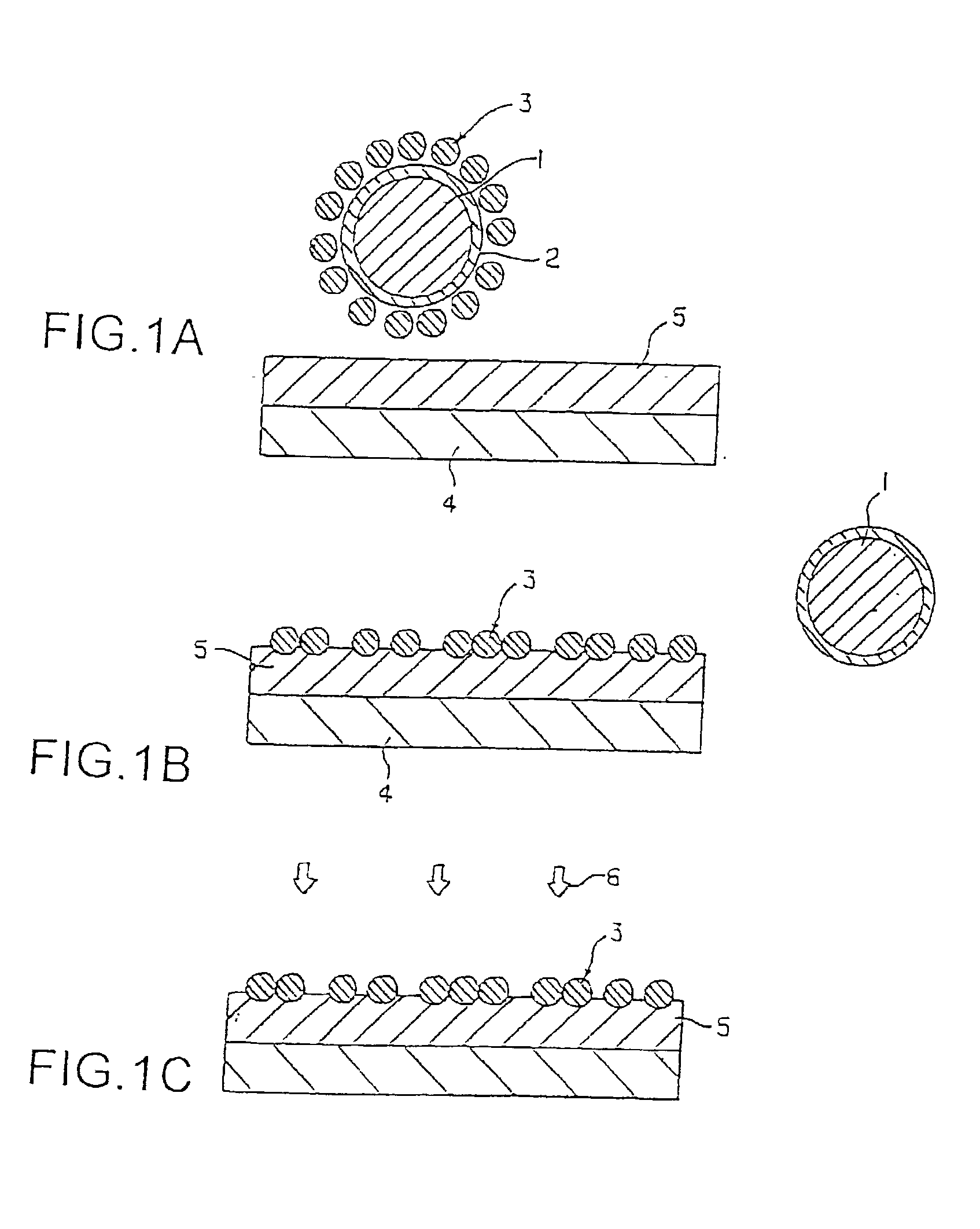
[0157] By using an alternate adsorption film forming method, an aqueous solution (dissolved in pure water) of polydiallyldimethyl ammonium chloride(PDDA) (20 mM) (monomer unit conversion) (made by Aldrich Co., Ltd., molecular weight: 100,000 to 200,000) and an aqueous solution (dissolved in pure water) of polystyrene sulfonate sodium salt (PSS) (20 mM) (monomer unit conversion) (made by Aldrich Co., Ltd., molecular weight: 70,000) were applied so that alternate adsorption films were formed on both of the surfaces of a glass substrate. The formation of the uppermost layer was carried out by using PDDA. (Formation of a single particle film: formation of a fine particle layer)

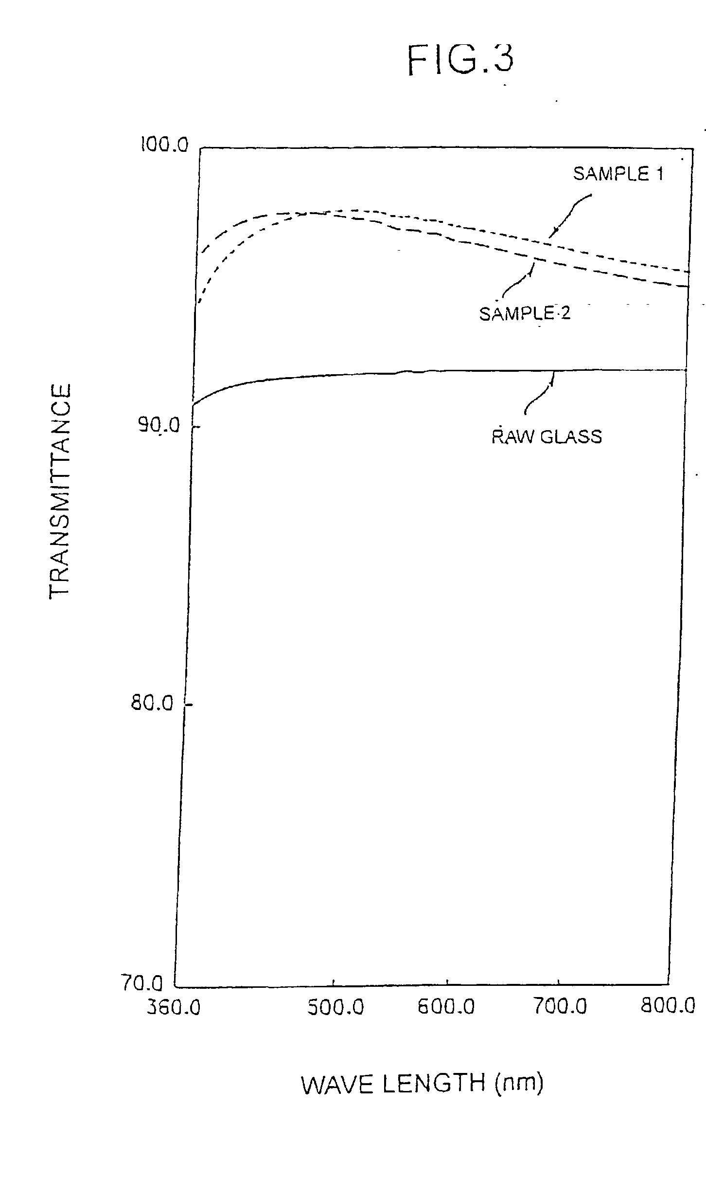
[0158] The above-mentioned base material was immersed in silica sol (made by Nissan Chemical Industries, Ltd.: Snow Tech ZL, particle size: 70 to 100 nm) for 30 seconds at room temperature, and then this was sufficiently cleaned, and dried t...

example 2

Charge Application to a Substrate: Formation of a Polymer Electrolyte Film

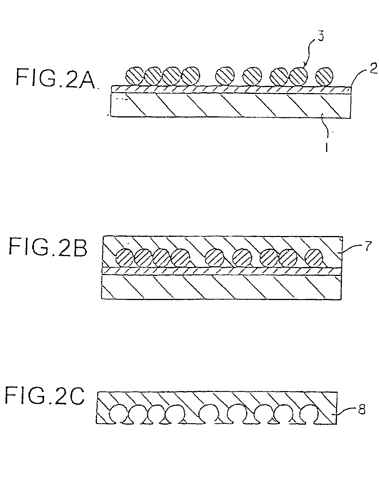
[0159] A cationic polymer electrolyte (made by Dai-Ichi Kogyo Seiyaku Co., Ltd., C-200H) ultra-thin film was formed on a surface of a glass substrate by a spin coating method.

Formation of a Single Particle Film: Formation of a Fine Particle Layer

[0160] By using the same silica sol as Example 1, and a single particle film was formed on one side face of a substrate in the same manner as Example 1; thus, sample 2 was prepared.

example 3

Charge Application to a Substrate: Formation of a Polymer Electrolyte Film

[0161] A tri-acetylated cellulose (TAC) film was processed for two minutes at 70.degree. C. in an aqueous solution of 2-normal potassium hydroxide, and the surface thereof was subjected to a hydrophilic-property-applying treatment. After the treatment, the TAC film was used so as to form an alternate adsorption film on the film surface by using an aqueous solution in which PDDA and PSS were dissolved in 0.1M NaCl solution at the same concentrations as Example 1.

Formation of a Single Particle Film: Formation of a Fine Particle Layer

[0162] By using the same materials as Example 1, the above-mentioned base material was processed in the same manner to prepare sample 3 on both of the surfaces of which single particle films were formed.


PUM

PropertyMeasurementUnit
thicknessaaaaaaaaaa
particle sizeaaaaaaaaaa
thicknessaaaaaaaaaa

Abstract

An objective of the present invention is to provide an antireflection film having a fine particle layer that is formed on a transparent substrate without allowing particles to aggregate as irregular lumps, while the region having no particles is being reduced to an area that is sufficiently small so as not to impair the visibility. In order to achieve the above-mentioned objective, the present invention provides an antireflection film that is characterized by having: a transparent substrate and a fine particle layer that is placed on the surface of the transparent substrate and made from at least a single layer of fine particles, wherein the surface of the transparent substrate and fine particles are allowed to adhere to each other by at least an electrostatic interaction, while the bulk of the above-mentioned fine particle layer is set to have a refractive index lower than the refractive index of the above-mentioned transparent substrate.

Description

[0001] The present invention relates to an antireflection film which is applicable to displays for personal-use and commercial-use, such as televisions, personal computers, word processors, mobile telephones and mobile information terminals by using systems such as CRTs (cathode ray tubes), LCDs (liquid crystal displays), plasma display and electro-luminescence, as well as to solar batteries, lenses, window glass in buildings, window glass for vehicles, curve mirrors, back mirrors and goggles, so as to improve the visibility, efficiency, etc. of these products, and also concerns a manufacturing method for such an antireflection film.[0002] With respect to a conventional manufacturing method for antireflection films, a method in which desired numbers of low refractive-index layers and high refractive-index layers are formed on a substrate with their thickness being controlled is widely used. However, this method generally requires a vacuum equipment, thereby failing to provide a meth...

Claims


Application Information

Patent Timeline
Patent Type & Authority Applications(United States)
IPC IPC(8): G02B5/02B32B7/02G02B1/11G02B1/111G02B1/16
CPCC03C17/007C03C2217/445C03C2217/465C03C2217/478C03C2217/77G02B1/11Y10T428/2998Y10T428/1086Y10T428/24893Y10T428/24942Y10T428/10Y10T428/24802Y10T428/25G02B1/113C09K2323/00C09K2323/06Y10T428/24995Y10T428/249952
Inventor HATTORI, HIDESHI
Owner DAI NIPPON PRINTING CO LTD
Why Eureka
Try Eureka