Semiconductor device and manufacturing method thereof

a technology of semiconductors and semiconductors, applied in non-linear optics, instruments, optics, etc., can solve the problems of gold structure not suitable for a circuit, large current (current flowing when the tft is in an off state), and large current in the off sta

Inactive Publication Date: 2002-11-28
SEMICON ENERGY LAB CO LTD
View PDF3 Cites 53 Cited by
  • Summary
  • Abstract
  • Description
  • Claims
  • Application Information

AI Technical Summary

Problems solved by technology

However, the TFT is considered as not so equal in terms of reliability to a MOSFET that is formed on a single crystal semiconductor substrate.
However, application of the GOLD structure (in this specification, a structure having an LDD region to which a gate voltage is applied is called a GOLD structure whereas a structure having only an LDD region to which a gate voltage is not applied is called an LDD structure) to a TFT has a problem that OFF current (current which flows when the TFT is in an OFF state) is larger compared to the LDD structure.
Therefore, the GOLD structure is not suitable for a circuit in which OFF current should be as small as possible, such as a pixel matrix circuit of an AM-LCD.

Method used


Image

  • Semiconductor device and manufacturing method thereof
  • Semiconductor device and manufacturing method thereof
  • Semiconductor device and manufacturing method thereof

Examples


embodiment 1

[0091] [Embodiment 1]

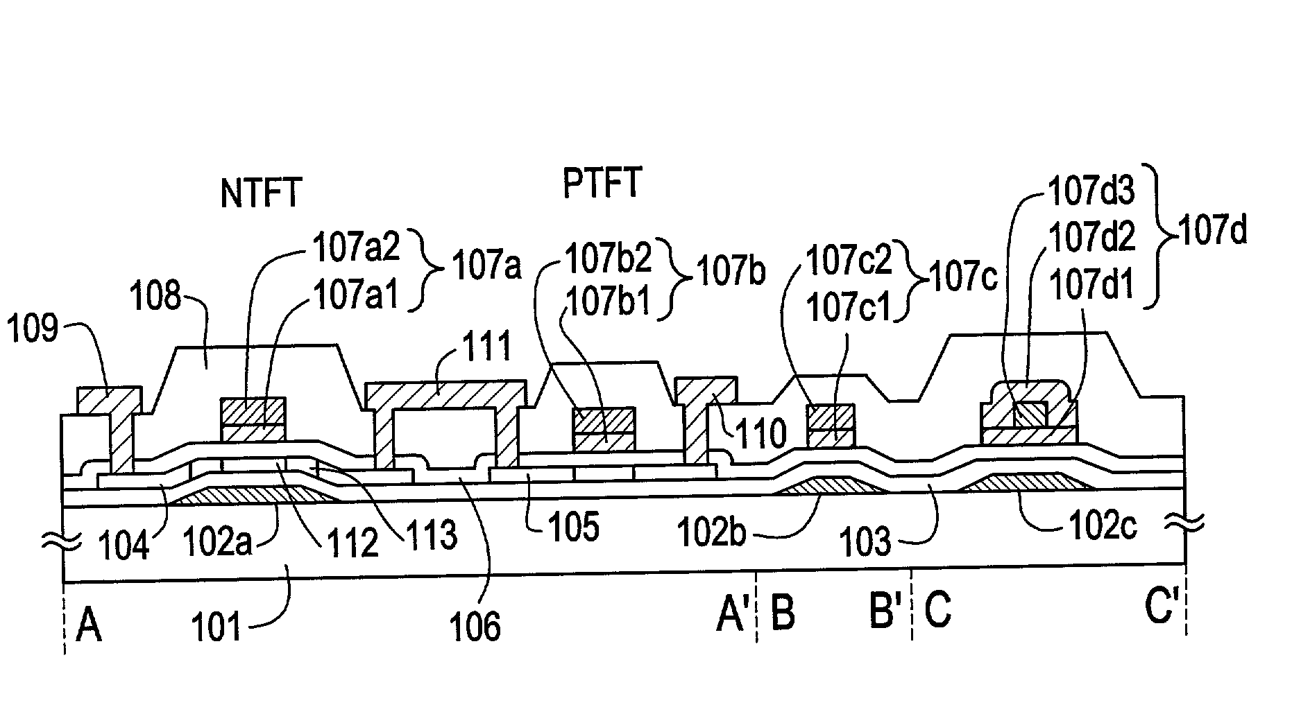
[0092] In this embodiment, a method of manufacturing the CMOS circuit described in Embodiment Mode 1 will be described. The description will be given with reference to FIG. 3.

[0093] First, a glass substrate is prepared as a substrate 301, and first wiring lines 302a, 302b, and 302c are formed thereon. The material of the first wiring lines is a laminated film, that a tungsten silicide (WSix) film and a silicon film are laminated in order by sputtering. The order of laminating can of course be reversed and the CVD method can be used as means of depositing. Further, it is effective to form oxide film on the surface after forming the above-mentioned laminated film in the sense of protection of the surface.

[0094] Other metal films, alloy films, or the like may of course be used as long as the first wiring lines 302a, 302b, and 302c are any film with conductivity. A chromium film or a tantalum film that can be formed into a pattern with a small taper angle is effecti...

embodiment 2

[0118] [Embodiment 2]

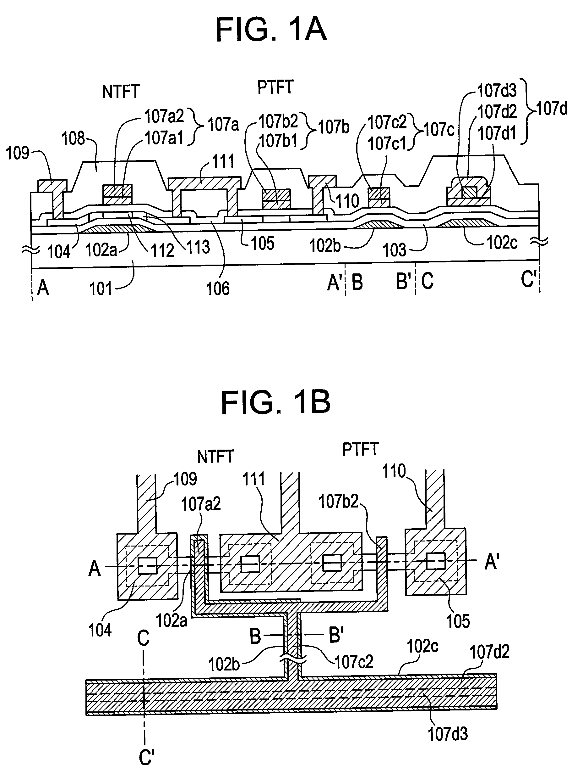
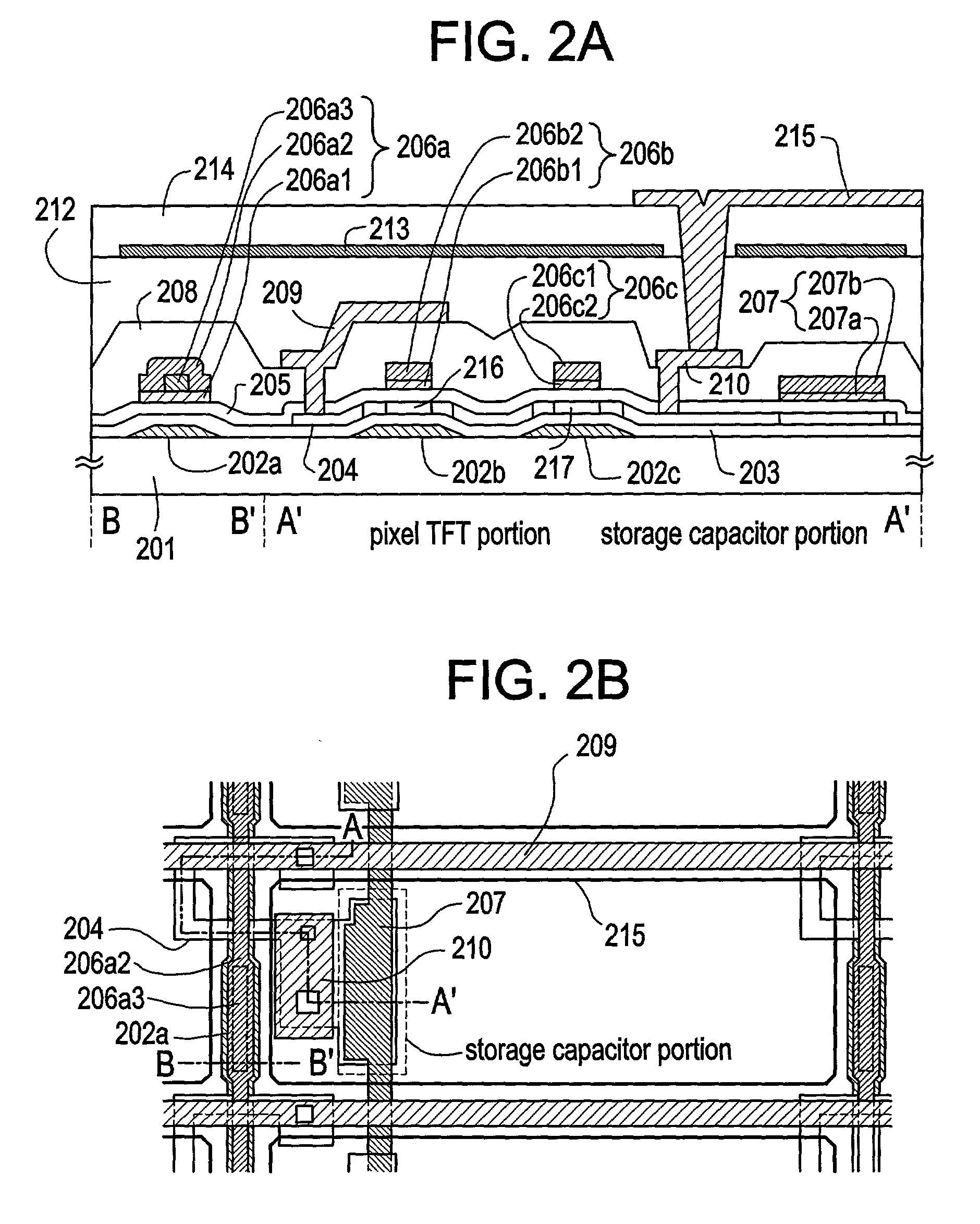
[0119] In this embodiment, a method of manufacturing the pixel matrix circuit described in Embodiment Mode 2 will be described. The description will be given with reference to FIGS. 4 and 5. The pixel matrix circuit is formed on the same substrate as the CMOS circuit shown in Embodiment 1 at the same time. Therefore, the description will be given in relation to the manufacturing process of Embodiment 1 and the same symbols as those in FIG. 3 are used when necessary.

[0120] First, second wiring lines 401a, 401b, and 401c are formed on the glass substrate 301. The second wiring lines have the material as described in Embodiment 1. Next, the first insulating layer 303, an active layer of a pixel TFT 402, the second insulating layer 306, the first conductive layer 307, a third conductive layer 403 and the second conductive layer 309 are formed consulting Embodiment 1. Thus obtained is the state of FIG. 4A. The CMOS circuit being formed simultaneously is now in the st...

embodiment 3

[0138] [Embodiment 3]

[0139] In this embodiment, an AM-LCD is provided with a pixel matrix circuit and a CMOS circuit (concretely, a driver circuit and signal processing circuit constructed of CMOS circuits) according to the present invention, and the appearance thereof is shown in FIG. 6.

[0140] On an active matrix substrate 601, a pixel matrix circuit 602, a signal line driving circuit (source driver circuit) 603, scanning line driving circuits (gate driver circuits) 604, and a signal processing circuit (including a signal divider circuit, a D / A converter circuit, and a .gamma. correction circuit) 605 are formed, and an FPC (flexible printed circuit) 606 is attached. Denoted by 607 is an opposite substrate.

[0141] The various circuits formed on the active matrix substrate 601 are illustrated in detail in a block diagram of FIG. 7.

[0142] In FIG. 7, 701 denotes a pixel matrix circuit that functions as an image display unit. 702a, 702b, and 702c represent a shift register circuit, a lev...


PUM

PropertyMeasurementUnit
sizeaaaaaaaaaa
diagonal sizeaaaaaaaaaa
thicknessaaaaaaaaaa

Abstract

In a CMOS circuit formed on a substrate 101, a subordinate gate wiring line (a first wiring line) 102a and main gate wiring line (a second wiring line) 107a are provided in an n-channel TFT. The LDD regions 113 overlaps the first wiring line 102a and does not overlap the second wiring line 107a. Thus, when a gate voltage is applied to the first wiring line, the GOLD structure is formed, while no applying forms the LLD structure. In this way, the GOLD structure and the LLD structure can be used appropriately in accordance with the respective specifications required for the circuits.

Description

[0001] 1. [Technical Field to Which the Invention Belongs][0002] The present invention relates to a semiconductor device having a circuit composed of a thin film transistor (hereinafter referred to as TFT). For example, the invention relates to an electro-optical device represented by a liquid crystal display panel and to electronic equipment mounted with the electro-optical device as a component.[0003] In this specification, a `semiconductor device` refers to a device in general that can function by utilizing semiconductor characteristics, and electro-optical devices, semiconductor circuits, and electronic equipment are semiconductor devices.[0004] 2. [Prior Art][0005] A thin film transistor (hereinafter referred to as TFT) can be formed on a transparent glass substrate, and hence its application to an active matrix liquid crystal display (hereinafter referred to as AM-LCD) has been developed actively. Since a TFT utilizing a crystalline semiconductor film (typically, a polysilicon...

Claims


Application Information

Patent Timeline
Patent Type & Authority Applications(United States)
IPC IPC(8): G02F1/136H01L29/786G02F1/1362G02F1/1368H01L21/336H01L21/77H01L21/84H01L27/12
CPCG02F1/13454H01L29/78648H01L29/78645H01L27/1214H01L27/124H01L27/1259
Inventor OHTANI, HISASHIYAMAZAKI, SHUNPEIKOYAMA, JUNARAI, YASUYUKI
Owner SEMICON ENERGY LAB CO LTD
Why Eureka
Try Eureka