
Method and apparatus for polishing metal and dielectric substrates

a dielectric substrate and metal technology, applied in the field of semiconductor device fabrication, can solve the problems of capacitative coupling between, affecting the functioning of semiconductor devices, and requiring processing capabilities,

Inactive Publication Date: 2003-02-13
APPLIED MATERIALS INC
View PDF0 Cites 48 Cited by
  • Summary
  • Abstract
  • Description
  • Claims
  • Application Information

AI Technical Summary

Problems solved by technology

However, as the fringes of circuit technology are pressed, the shrinking dimensions of interconnects in VLSI and ULSI technology has placed additional demands on the processing capabilities.
Increased capacitative coupling between layers can detrimentally affect the functioning of semiconductor devices.
One difficulty in using copper in semiconductor devices is that copper is difficult to etch and achieve a precise pattern.
Etching with copper using traditional deposition / etch processes for forming interconnects has been less than satisfactory.
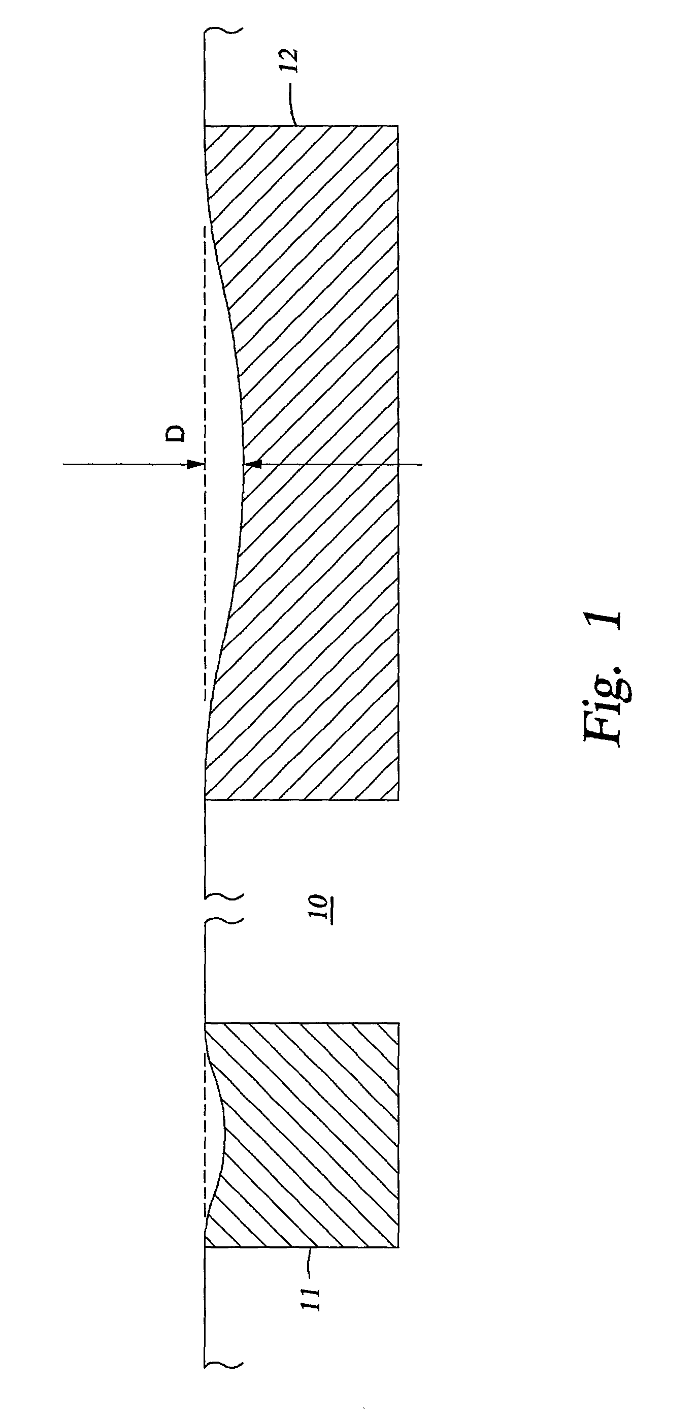
However, conventional polishing processes often result in uneven removal of the copper features and the dielectric layer resulting is the formation of topographical defects, such as concavities or depressions in the copper features, referred to as dishing, and excess removal of dielectric material surrounding the copper features, referred to as erosion.
Dishing results in a non-planar surface that impairs the ability to print high-resolution lines during subsequent photolithographic steps and detrimentally affects subsequent surface topography of the substrate and device formation.
Dishing also detrimentally affects the performance of devices by lowering the conductance and increasing the resistance of the devices, contrary to the benefit of using higher conductive materials, such as copper.
An additional difficulty also arises when using low k dielectric material in copper dual damascene formation.
Low k dielectric materials are typically soft, porous, and brittle.
Current polishing pressures, about 4 psi or greater, can damage the low k dielectric material and form defects in the substrate surface such as film delamination due to high shear stress caused by the friction between the polishing pad and substrate surface.
However, polishing substrates at reduced pressures often results in less than desirable polishing rates, non-uniform polishing, and less than desirable planarization of the substrate surface.
Such undesirable processing of the substrate surface may also result in reduced substrate throughput and less than desirable polish quality of the substrate surface.
Additionally, low polishing pressure processes may be unable to sufficiently remove all of the desired copper materials from a substrate surface such as at the interface between copper and the barrier layer, which is generally non-planar.
The remaining copper materials, or residues, can detrimentally affect device formation, such as creating short-circuits within or between devices, reduce device yields, reduce substrate throughput, and detrimentally affect the polish quality of the substrate surface.
However, it is believed that the corners or edges of the patterns formed in the polishing pad surface may perform as a "blade" or cutting surface that may damage low k dielectric films and increase surface friction during polishing, which can lead to increased film delamination, and that a pattern-free, i.e., corner-free, polishing pad is typically used when polishing substrates with the processes described herein.
However, it is believed that the seams of between the polishing pad material and the transparent material also form corners or grooves in the surfaces of the polishing pads.
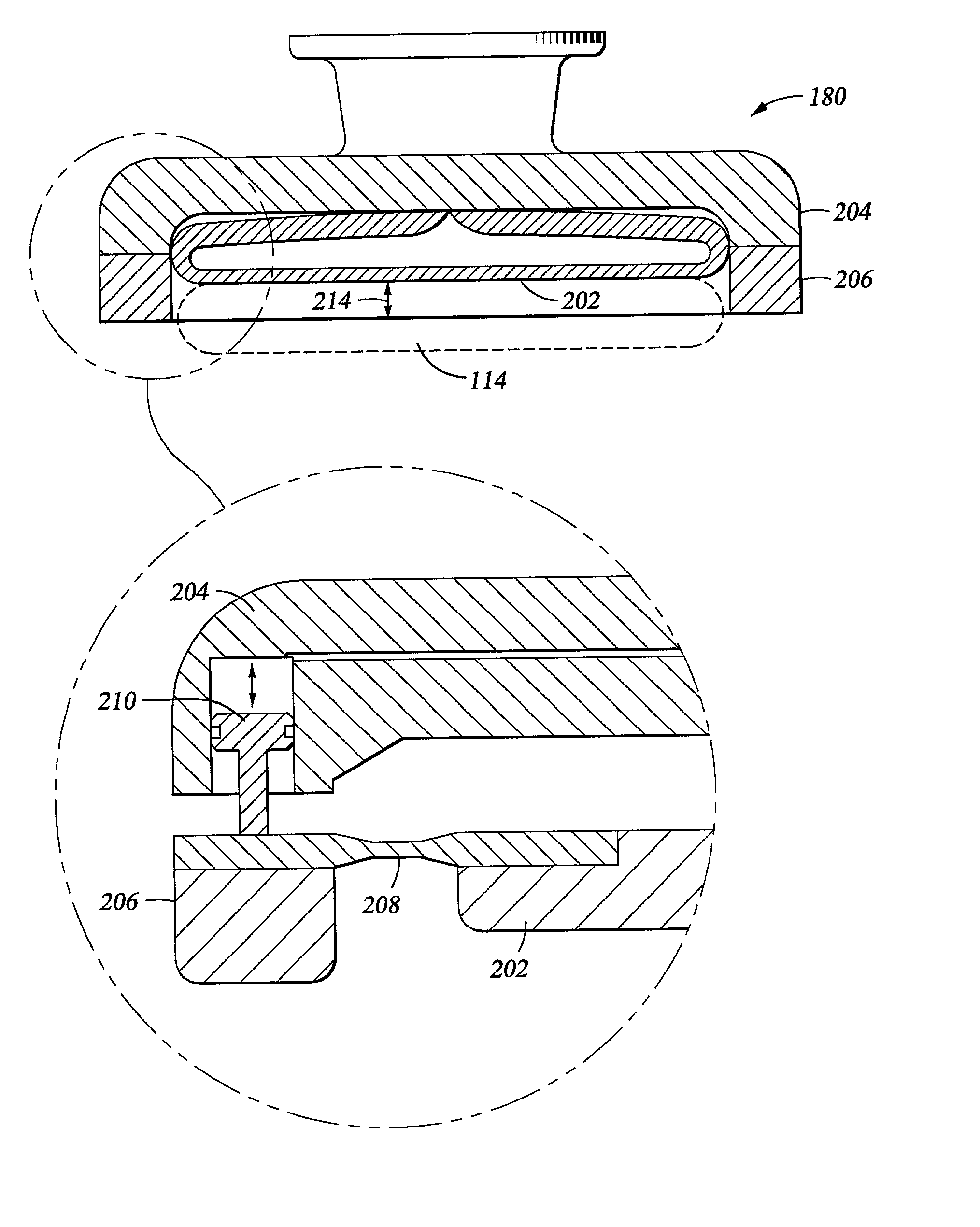
A retaining ring pressure between 3 and about 6 psi greater than the membrane pressure has been used to polish substrates and has been observed to result in substrates with minimal film damage and delamination.
Low k dielectric materials are particularly sensitive to friction from shear forces, and the reduced friction reduces the force that may damage low k films and result in delamination.
It is further believed that the rotational speeds described herein and the ratio of rotational speeds provide a relative linear velocity to the substrate surface, which results in removal of residual conductive materials with reduced non-uniformity, further enhanced by reduced polishing composition flow rates, compared to previous polishing processes.

Method used


Image

  • Method and apparatus for polishing metal and dielectric substrates
  • Method and apparatus for polishing metal and dielectric substrates
  • Method and apparatus for polishing metal and dielectric substrates

Examples


Embodiment Construction

:

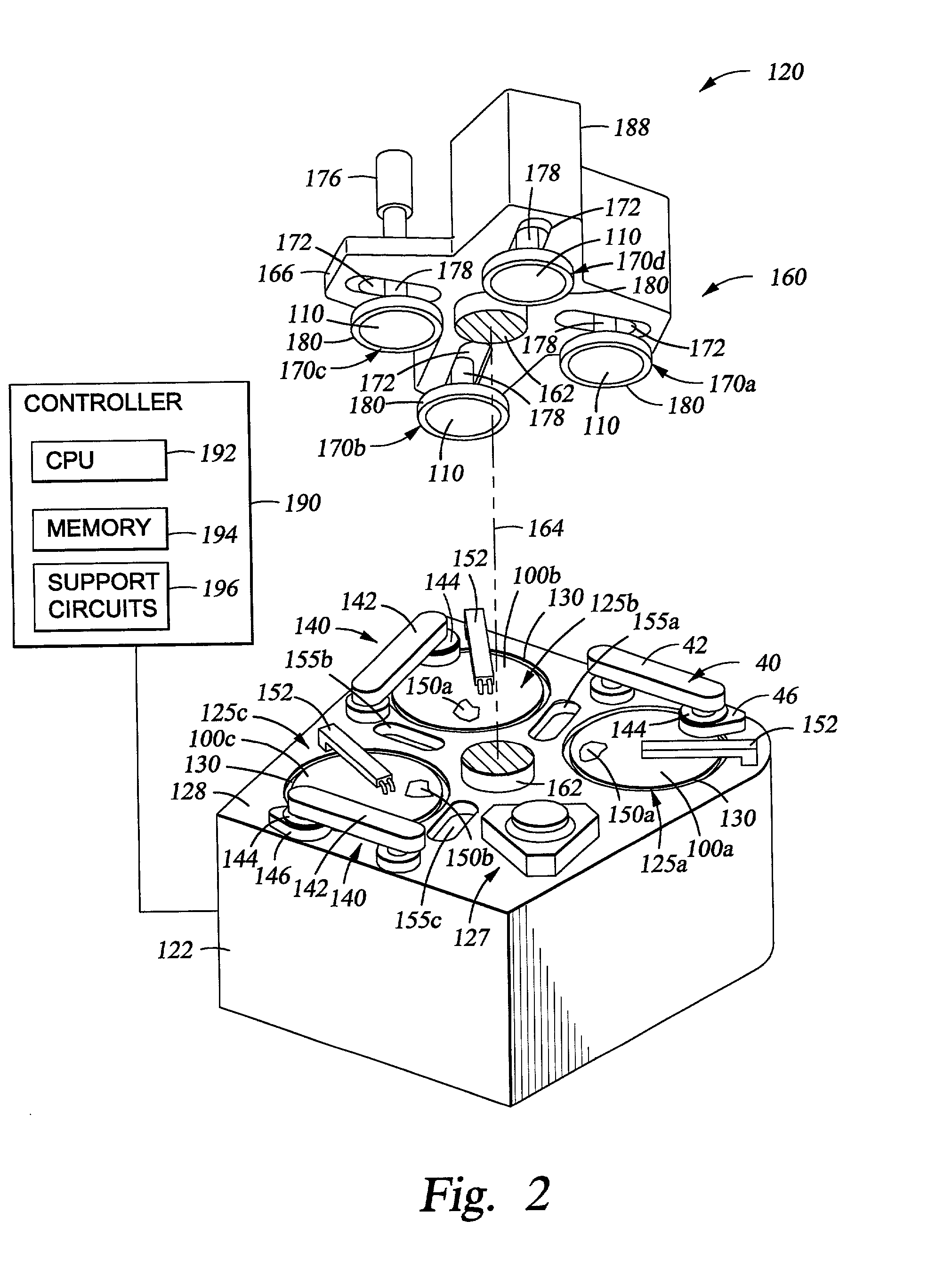
[0106] A series of substrates were polished according to the two-step polishing process described above in steps 300-350. A first experimental process was performed on a Mirra.TM. three platen polishing system using Cabot EPC-5001 composition on a IC-1010 polishing pad on platen 1, an Electrapolish.TM. polishing composition from Applied Materials, Inc., of Santa Clara, Calif., on a IC-1010 on platen 2, and an Electrapolish.TM. polishing composition on a Politex pad on platen 3.

[0107] The substrates polished under the processing condition shown in Table 1 below comprise a substrate stack of silicon, a first Black Diamond.TM. low k dielectric film, a BLOk.TM. low k dielectric film, a second Black Diamond.TM. low k dielectric film, a dielectric anti-reflective coating (DARC), which a feature definition was formed in the dielectric layers and filled using a tantalum nitride barrier layer, and then a copper fill of the feature definition. An example substrate may contain a silicon surfa...


PUM

PropertyMeasurementUnit
Pressureaaaaaaaaaa
Pressureaaaaaaaaaa
Pressureaaaaaaaaaa

Abstract

Method and apparatus are provided for polishing substrates comprising conductive and low k dielectric materials with reduced or minimum substrate surface damage and delamination. In one aspect, a method is provided for processing a substrate including positioning a substrate having a conductive material formed thereon in a polishing apparatus having one or more rotational carrier heads and one or more rotatable platens, wherein the carrier head comprises a retaining ring and a membrane for securing a substrate and the platen has a polishing article disposed thereon, contacting the substrate surface and the polishing article to each other at a retaining ring contact pressure of about 0.4 psi or greater than a membrane pressure, and polishing the substrate to remove conductive material.

Description

[0001] This application claims benefit of United States provisional patent application serial No. 60 / 304,543, filed Jul. 11, 2001, which is herein incorporated by reference.[0002] 1. Field of the Invention[0003] Aspects of the invention generally relate to the fabrication of semiconductor devices and to chemical mechanical polishing and planarization of semiconductor devices.[0004] 2. Description of the Related Art[0005] Reliably producing sub-half micron and smaller features is one of the key technologies for the next generation of very large scale integration (VLSI) and ultra large-scale integration (ULSI) of semiconductor devices. However, as the fringes of circuit technology are pressed, the shrinking dimensions of interconnects in VLSI and ULSI technology has placed additional demands on the processing capabilities. The multilevel interconnects that lie at the heart of this technology require precise processing of high aspect ratio features, such as vias, contacts, lines, and o...

Claims


Application Information

Patent Timeline
IPC IPC(8): B24B1/00B24B5/00B24B29/00B24B37/04C23F1/00H01L21/306H01L21/321H01L21/461H01L21/4763H01L21/768
CPCB24B37/042B24B37/30H01L21/3212H01L21/7684
Inventor MOON, YONGSIKMAI, DAVIDWIJEKOON, KAPILABAJAJ, RAJEEVSURANA, RAHULHU, YONGQIKAUSHAL, TONY S.LI, SHIJIANLI, JUI-LUNGWANG, SHI-PINGLAM, GARYREDEKER, FRED C.
Owner APPLIED MATERIALS INC
Learn More