Semiconductor light emitting device

a technology of semiconductors and light emitting devices, which is applied in the direction of solid-state devices, basic electric elements, transportation and packaging, etc., can solve the problems of reducing the external quantum efficiency of the device, attenuating the light, and unable to effectively emit to the outside,

Inactive Publication Date: 2003-03-27
NICHIA CORP
View PDF2 Cites 233 Cited by
  • Summary
  • Abstract
  • Description
  • Claims
  • Application Information

AI Technical Summary

Problems solved by technology

Therefore, the emitted light is attenuated and cannot be effectively emitted to the outside, which lowers the external quantum efficiency of the device.
However, it is difficult to make such a chip.
However, with such a method, there is a risk that the p-n junction may be partially damaged and the effective light emitting region is reduced.
In addition, if the light absorption within the light guide is so large, the external quantum efficiency does not reach a sufficient level only with the randomly roughed surface.
This lowers the efficiency of the light emission.
If a cavity is remained around the protrusions or recesses, the scattering or diffracting effects are prevented, which lowers the output power of the device.
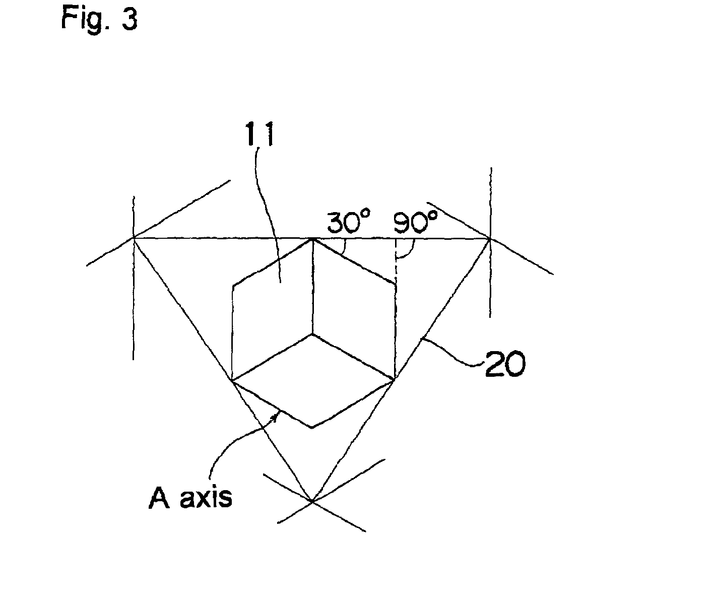
In the case that the recesses and / or protruding portions have, as component sides, lines approximately parallel to the stably growing face of the semiconductor, crystal defects occur in such portions at the time of the film growth of the semiconductor layer and these defects lower the internal quantum efficiency which causes the lowering of the external quantum efficiency.
However, the depths of the recesses or the steps of protruding portions becomes larger than the thickness of the semiconductor layer, which is made to grow on the substrate, it becomes difficult for a current to flow in the lateral direction within the layered structure so that the efficiency of the light emission is lowered.
On the other hand, too large taper angle decreases a scattering efficiency and induces pits in semiconductor layers.
Second, in a device having the unevenness on the substrate, light that inherently propagates laterally or downwardly is scattered or diffracted to go upwardly.
However, if a conventional transparent electrode is formed to cover the entire surface of the device, the scattered or diffracted light is partly absorbed and weakened by the electrode.
On the other hand, too large taper angle decreases a scattering efficiency and induces pits in semiconductor layers.
However, at the time when light propagates within the light guide formed in the structure of a light emitting electrode-semiconductor layer-substrate, emitted light is absorbed or attenuated by not only the semiconductor layer but, also, by the light transmitting electrode and by the substrate as a result of the effects of "leakage" of reflected light.
Though the upper limit is not specifically set, in actuality when L / S becomes greater than 1 .mu.m / .mu.m.sup.2, the size of one opening becomes too small and the device becomes impractical.
In the case that the angle of taper is 30 degrees or less, the resistance value of the p-side ohmic electrode becomes great in the tapered portion and therefore, it becomes difficult to effectively utilize the property that the peripheral portion of the electrode emits intense light.

Method used


Image

  • Semiconductor light emitting device
  • Semiconductor light emitting device
  • Semiconductor light emitting device

Examples


example 2

[0111] A sapphire substrate, of which a C plane (0001) is used as the main surface, having the orientation flat in an A plane (11-20) is used as the substrate.

[0112] A process in the substrate and layering of an n-type semiconductor layer to a p-type semiconductor layer are carried out in the same manner as in first example.

[0113] Next, a p-type semiconductor layer made of Mg doped GaN, an active layer and a portion of the n-type semiconductor layer are etched in order to form an n electrode so that the n-type semiconductor layer made of Si doped GaN is exposed.

[0114] Next, a photomask having a pattern wherein equilateral triangles having a side of 5 .mu.m, as shown in FIG. 16, are most densely filled per unit area is utilized so that a light transmitting p electrode made of Ni / Au is formed on almost the entirety of the surface of the p-type semiconductor layer.

[0115] Furthermore, a p-side pad electrode made of Au is formed at a position opposite to the exposed surface of the n-type...

example 3

[0118] A sapphire substrate, of which a C plane (0001) is used as the main surface, having the orientation flat in an A plane (11-20) is used as the substrate.

[0119] A process of the substrate and layering of an n-type semiconductor layer to a p-type semiconductor layer are carried out in the same manner as in first example.

[0120] Next, starting from Mg doped GaN, the p-type semiconductor layer, an active layer and a portion of the n-type semiconductor layer are etched in order to form an n electrode so that the Si doped GaN layer is exposed.

[0121] Next, a photomask of a square pattern is utilized so as to form a p electrode 104 made of Rh on almost the entirety of the surface of the p-type semiconductor layer. The shape of the openings is square, of which side is 7.7 .mu.m. The interval of the openings is 6.3 .mu.m. The aperture ratio of the opening is about 30%.

[0122] Furthermore, a p-side pad electrode made of Pt / Au is formed at a position opposite to the exposed surface of the n...

example 4

[0125] In the light emitting device of third example, p electrode is formed in a stripe form, as shown in FIGS. 14C. By adopting such a stripe electrode structure, a current supplied from a p-side pad electrode to semiconductor layer is made uniform within the surface to increase the efficiency of the light emission.

[0126] The stripes of the first electrode are created as openings that expose semiconductor layer and therefore, the length of the edge of the electrode can be significantly increased and as a result, the efficiency of the light emission is increased. At this time, it is preferable to achieve L / S.gtoreq.0.024 .mu.m / .mu.m.sup.2 wherein the value of S is gained by adding the total area Sa of openings 5 corresponding to the plurality of stripes, which exposes semiconductor layer, and area Sb of the electrode portion that does not expose semiconductor layer, and the value of L is the total sum of the length of the circumferences of openings 5.


PUM


Abstract

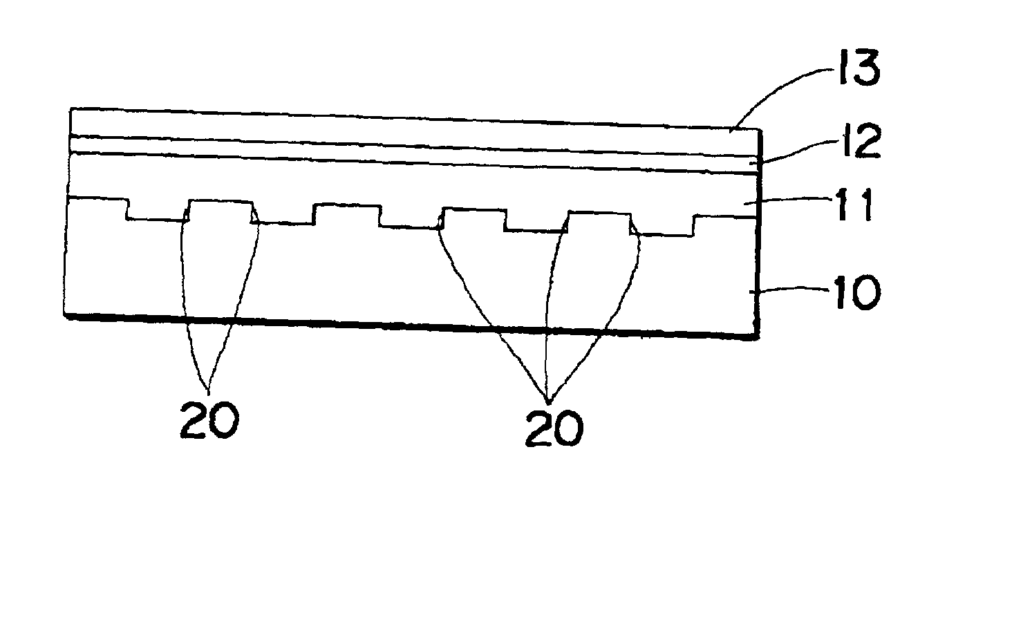
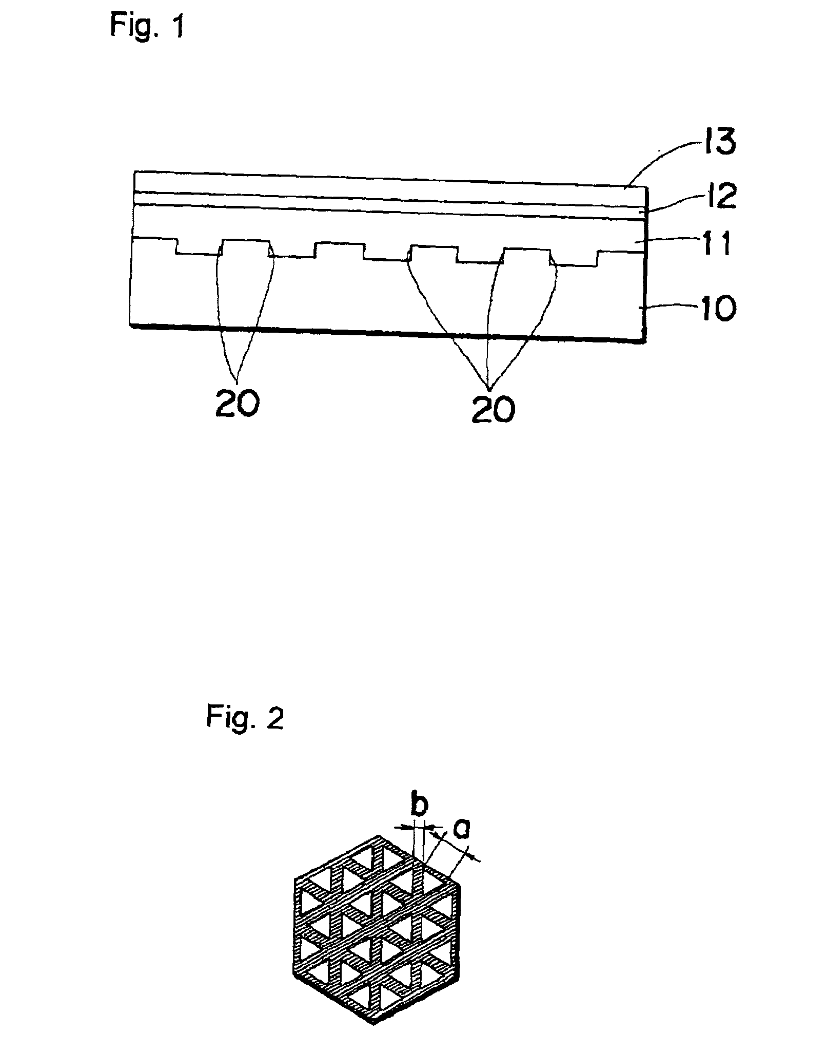
A high external quantum efficiency is stably secured in a semiconductor light emitting device. At least one recess and/or protruding portion is created on the surface portion of a substrate for scattering or diffracting light generated in a light emitting region. The recess and/or protruding portion has a shape that prevents crystal defects from occurring in semiconductor layers.

Description

[0001] The present invention relates to a semiconductor light emitting device, in particular, to a nitride-based compound semiconductor light emitting device wherein a recess or a protruding portion is provided in a substrate so that defects do not occur in the semiconductor and thereby, the direction of guided light is changed in a semiconductor layer to increase the external quantum efficiency.DESCRIPTION OF THE PRIOR ART[0002] In a semiconductor light emitting device, for example, in a light emitting diode (LED), an n-type semiconductor layer, a light emitting region and a p-type semiconductor layer are essentially made to grow on top of a substrate to form a layered structure while a structure is adopted wherein electrodes are formed on the p-type semiconductor layer and on the n-type semiconductor layer. Light, generated through recombination of holes and electrons that have been injected through the semiconductor layers to the light emitting region, is emitted through a light ...

Claims


Application Information

Patent Timeline
Patent Type & Authority Applications(United States)
IPC IPC(8): H01L33/38H01L33/00H01L33/22H01L33/24H01L33/32H01L33/42
CPCH01L33/007H01L33/20H01L33/22H01L33/24Y10T428/24355H01L33/26H01L33/16Y10T428/24479H01L2933/0083H01L21/02378H01L21/0254H01L21/02647H01L33/38H01L33/32
Inventor NIKI, ISAMUYAMADA, MOTOKAZUSANO, MASAHIKOSHIOJI, SHUJI
Owner NICHIA CORP
Why Eureka
Try Eureka