Semiconductor device and manufactruing method therefor

Active Publication Date: 2003-04-17
HITACHI LTD
View PDF0 Cites 7 Cited by
  • Summary
  • Abstract
  • Description
  • Claims
  • Application Information

AI Technical Summary

Benefits of technology

0029] Herein, a description was directed to both of the cases where the SOI substrate with the 1.5-.mu.m thick silicon layer has the 0.5-.mu.m thick buried oxide film and the 3.0-.mu.m buried oxide film. In both of the cases, the effect of the improved breakdown voltage was obtained. As a matter of course, the thickness of the silicon layer may be set to any value more or less than 1.5 .mu.m. Similarly, the thickness of the buried oxide film may also be set to any value. The effect of the improved breakd

Problems solved by technology

However, when the buried insulating film becomes thick, a warp in a wafer increases in the manufacturing process of the device.
Consequently, the process at the final stage in completion of the device cannot be performed.
However, if the thickness of the silicon layer is increased, it takes much time to form trenches required for isolation of a device-forming region.
For this reason, throughput is reduced, so that a cost problem arises.
In addition, it becomes difficult to form a completely vertical deep trench and cover the trench with an insulated film tightly.
Accordingly, if the high concentration N-type layer is present in the silicon layer with its thickness reduced, a high breakdown voltage cannot be obtained.
When the concentration of the substrate becomes high, even if the drain-source distance is increased, the depletion layer formed between the p-body layer and the N-

Method used


Image

  • Semiconductor device and manufactruing method therefor
  • Semiconductor device and manufactruing method therefor
  • Semiconductor device and manufactruing method therefor

Examples


first embodiment

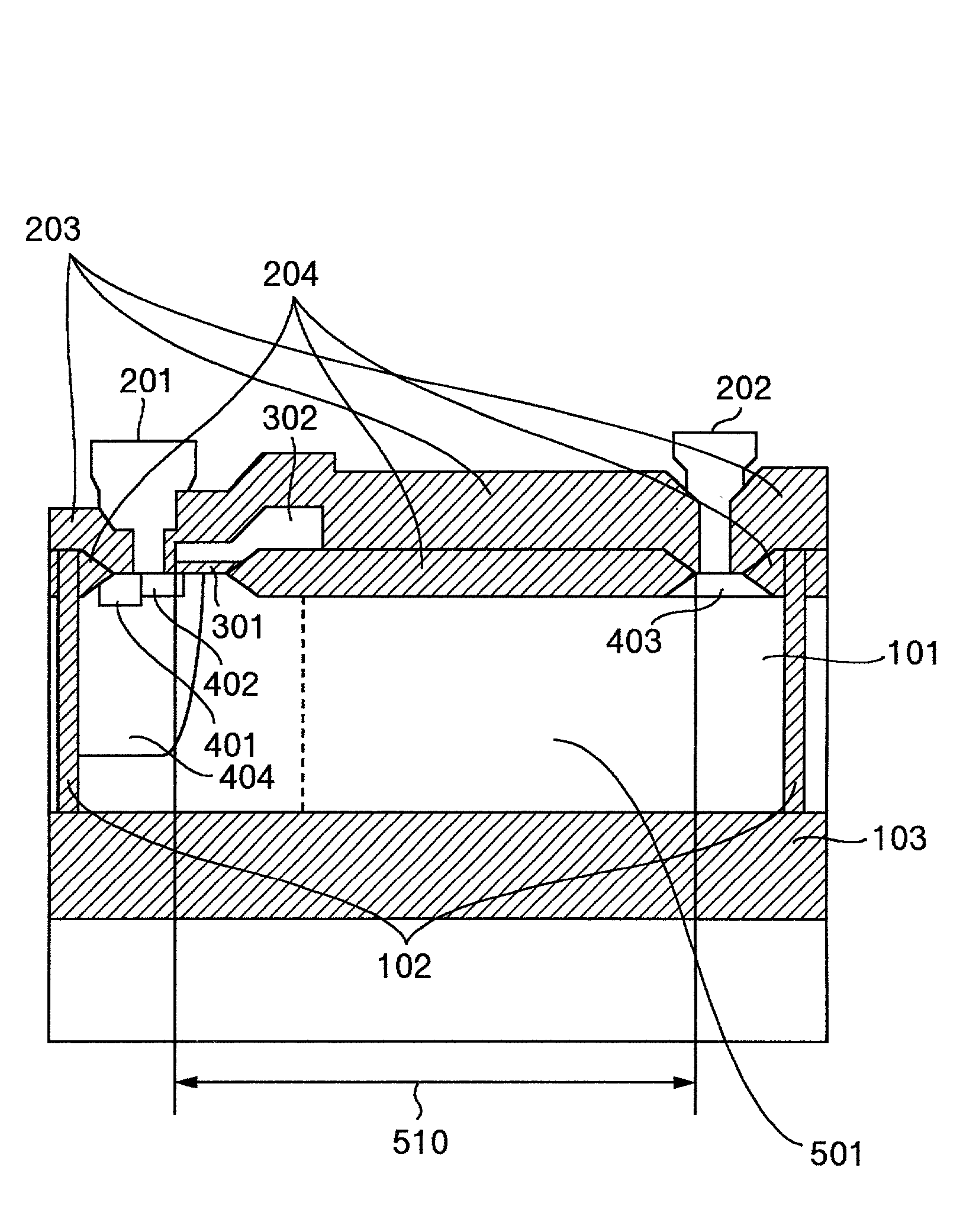
[0050] First, FIG. 1 shows a semiconductor device according to the present invention, and is a vertical sectional view illustrating the structure of an N-channel MOS field-effect transistor. The N-channel MOS field-effect transistor comprises the source electrode 201, and the drain electrode 202 and gate electrode 302 disposed in a lateral direction via the field oxide film 204, on the SOI substrate 101 having the N-type device-forming region. The transistor further comprises the gate oxide film 301, high concentration P-type layer 401, high concentration N-type layer 402, high concentration N-type layer 403, and p-type layer or p-body layer 404. The gate oxide film 301 is in contact with the gate electrode 302. The high concentration P-type layer 401 is in contact with the source electrode 201, and the high concentration N-type layer 402 is in contact with the source electrode 201 and the gate oxide film 301. The high concentration N-type layer 403 is in contact with the drain elec...

second embodiment

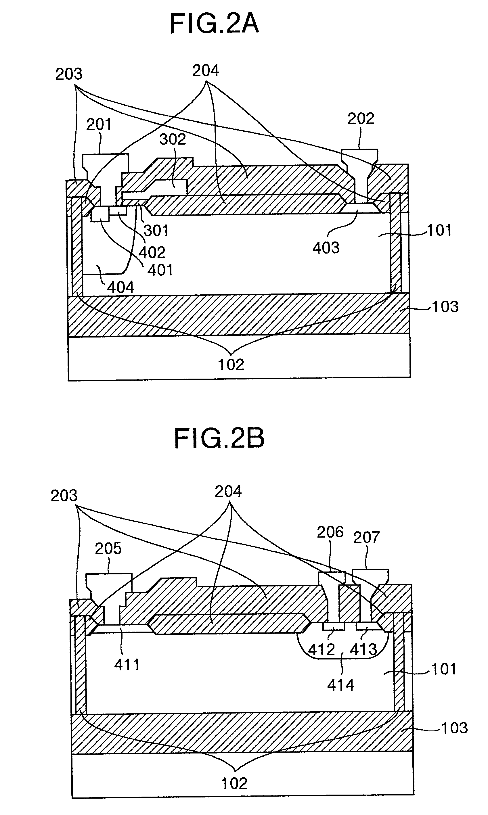
[0052] FIG. 4 shows a semiconductor device according to the present invention, and is a vertical sectional view illustrating the structure of an NPN bipolar transistor. The NPN bipolar transistor comprises the collector electrode 205, and the base electrode 206 and the emitter electrode 207 disposed in the lateral direction via the field oxide film 204, on the SOI substrate 101 having the N-type device-forming region. The transistor further comprises the high concentration N-type layer 411, high concentration P-type layer 412, high concentration N-type layer 413, and p-type base layer 414. The high concentration N-type layer 411 is in contact with the collector electrode 205. The high concentration P-type layer 412 is in contact with the base electrode 206. The high concentration N-type layer 413 is in contact with the emitter electrode 207. The P-type base layer 414 is in contact with the high concentration p-type layer 412 and the high concentration N-type layer 413. This transist...

third embodiment

[0054] FIG. 5 shows a semiconductor device according to the present invention, and is a vertical sectional view illustrating an N-channel MOS field-effect transistor. The N-channel MOS field-effect transistor comprises the source electrode 201, and the drain electrode 202 and the gate electrode 302 disposed in the lateral direction via the field oxide film 204, on the SOI substrate having the N-type device-forming region. The transistor further comprises the gate oxide film 301 in contact with the gate electrode 302, high concentration P-type layer 401, high concentration N-type layer 402, high concentration N-type layer 403, and p-type layer or p-body layer 404. The high concentration P-type layer 401 is in contact with the source electrode 201. The high concentration N-type layer 402 is in contact with the source electrode 201 and the gate oxide film 301. The high concentration N-type layer 403 is in contact with the drain electrode 202. The p-body layer 404 is in contact with the...


PUM


Abstract

An N-channel MOS field-effect transistor on an SOI substrate including a source electrode, drain and gate electrodes both disposed via a field oxide film, a gate oxide film, a high concentration P-type layer, a high concentration N-type layer contacting the source electrode and the gate oxide film, a high concentration N-type layer contacting the drain electrode, a p-body layer contacting the high concentration P-type and N-type layers and the gate oxide film. In this transistor, an N-type layer with a concentration higher than that of a drain region contacting the p-body layer constitutes a region covering at most 95% of the source-drain distance. Further, an N-type region having a concentration from 3.times.10.sup.16/cm.sup.3 to 1.times.10.sup.22/cm.sup.3 is provided near a buried oxide film under the drain electrode.

Description

BACKGROUND OF THE INVENTION[0001] The present invention relates to a semiconductor device and a method of manufacturing the semiconductor device. More specifically, the invention relates to an insulated-gate field-effect transistor and a bipolar transistor, both formed on an SOI substrate.[0002] In a high breakdown voltage semiconductor device formed on the SOI (Silicon On Insulator) substrate, the magnitude of the breakdown voltage of the device determines the thickness of a silicon layer and the thickness of a buried insulating film. The silicon layer is the active region where the device is formed, and is formed over a support silicon substrate via the insulating film. The breakdown voltage of an N-channel insulated-gate field-effect transistor is herein defined as a voltage applied to a drain electrode therein when an electric current flowing through the drain electrode has become 10 .mu.A through the application of the voltage to the drain electrode. In this case, the gate widt...

Claims


Application Information

Patent Timeline
IPC IPC(8): H01L21/331H01L21/336H01L21/762H01L21/77H01L21/8222H01L21/8248H01L21/8249H01L21/84H01L27/06H01L27/08H01L27/12H01L29/08H01L29/10H01L29/73H01L29/78H01L29/786H04M3/00H04M3/18
CPCG09G3/28H01L29/66681H01L21/76283H01L21/84H01L27/1203H01L29/0847H01L29/1083H01L29/66265H01L29/66674H01L29/7317H01L29/7824H04M3/005H04M3/18H04M2201/06H01L21/76264
Inventor OHYANAGI, TAKASUMIWATANABE, ATSUO
Owner HITACHI LTD
Why Eureka
Try Eureka