Photovoltaic device

a photovoltaic device and photovoltaic cell technology, applied in the field of photovoltaic devices/cells, can solve the problems of increasing non-radiative recombination, reducing the efficiency of photovoltaic generation,

Inactive Publication Date: 2003-05-15
IMPERIAL INNOVATIONS LTD
View PDF0 Cites 75 Cited by
  • Summary
  • Abstract
  • Description
  • Claims
  • Application Information

AI Technical Summary

Benefits of technology

[0008] With this concept one can extend the absorption threshold to longer wavelength without introducing dislocations.
[0009] With a strain-balanced multi-quantum-well stack in the intrinsic region of a two-terminal photovoltaic device the absorption threshold can be extended to longer wavelengths. In particular, with high bandgap barriers the dark current can be reduced at the same time, and hence the conversion efficiency is increased significantly.
[0010] What is also helpful to achieve higher conversion efficiencies is an improved voltage performance, due to a lower dark current. This is provided by the higher barriers which may also be provided when balancing the strain.
[0014] This combination of layers allows provision of an advantageously high barrier energy within the multiple quantum well system which reduces the dark current. Furthermore, this composition is well suited to stress balancing and use with the above mentioned virtual substrate.

Problems solved by technology

Appropriate and inexpensive substrates of the required lattice constant and band-gap are not available, so the lower band-gap material is often strained to the substrate, introducing dislocations which increase non-radiative recombination.
Freundlich et al. have proposed strained quantum well devices [U.S. Pat. No. 5,851,310 (1998), U.S. Pat. No. 6,150,604 (2000)], but these can only incorporate a restricted number of wells without creating dislocations.
Freundlich proposes limiting the number of wells to a maximum of 20, which will not produce sufficient absorption for efficient generation however.
A device providing an average lattice constant matching the substrate may still allow a significant build up of stress that will result in undesirable dislocations.

Method used


Image

  • Photovoltaic device
  • Photovoltaic device
  • Photovoltaic device

Examples


Embodiment Construction

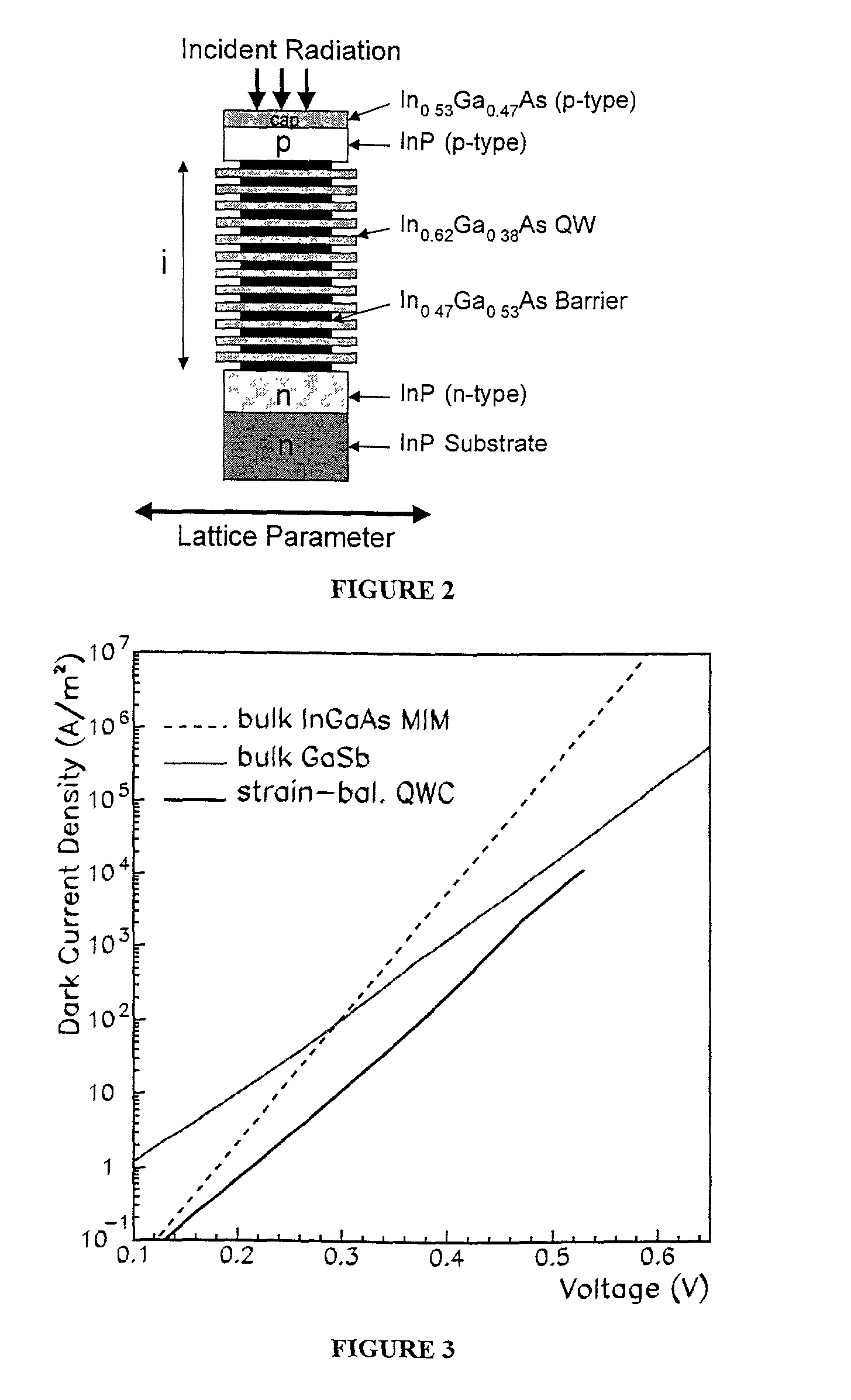
[0025] As an example for a strain-compensated QWC, we consider a 30 well In.sub.0.62Ga.sub.0.38As / In.sub.0.47Ga.sub.0.53As (InP) QWC, grown by MOVPE, whose sample description is given in Table I.

1TABLE I Sample description of a strain-compensated quantum well cell. Conc. Layers Thickness (.ANG.) Material Function Doping (cm.sup.-3) 1 1000 In.sub.0.53Ga.sub.0.47As Cap p 1E + 19 1 7000 InP Emitter p 2E + 18 30 120 In.sub.0.45Ga.sub.0.55As Barrier i 30 120 In.sub.0.62Ga.sub.0.38As Well i 1 120 In.sub.0.47Ga.sub.0.53As Barrier i 1 5000 InP Base n 1E + 18 InP Substrate n

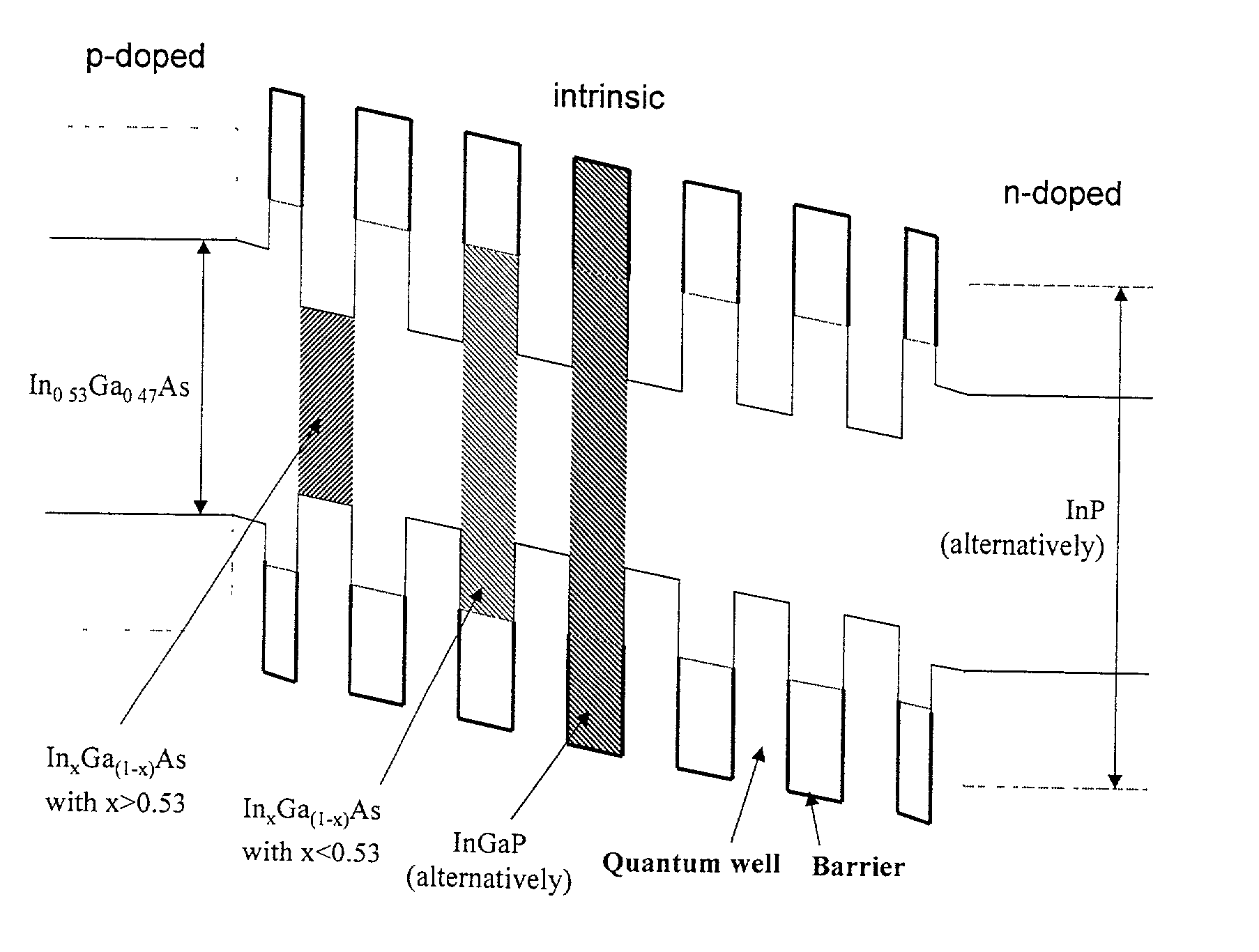
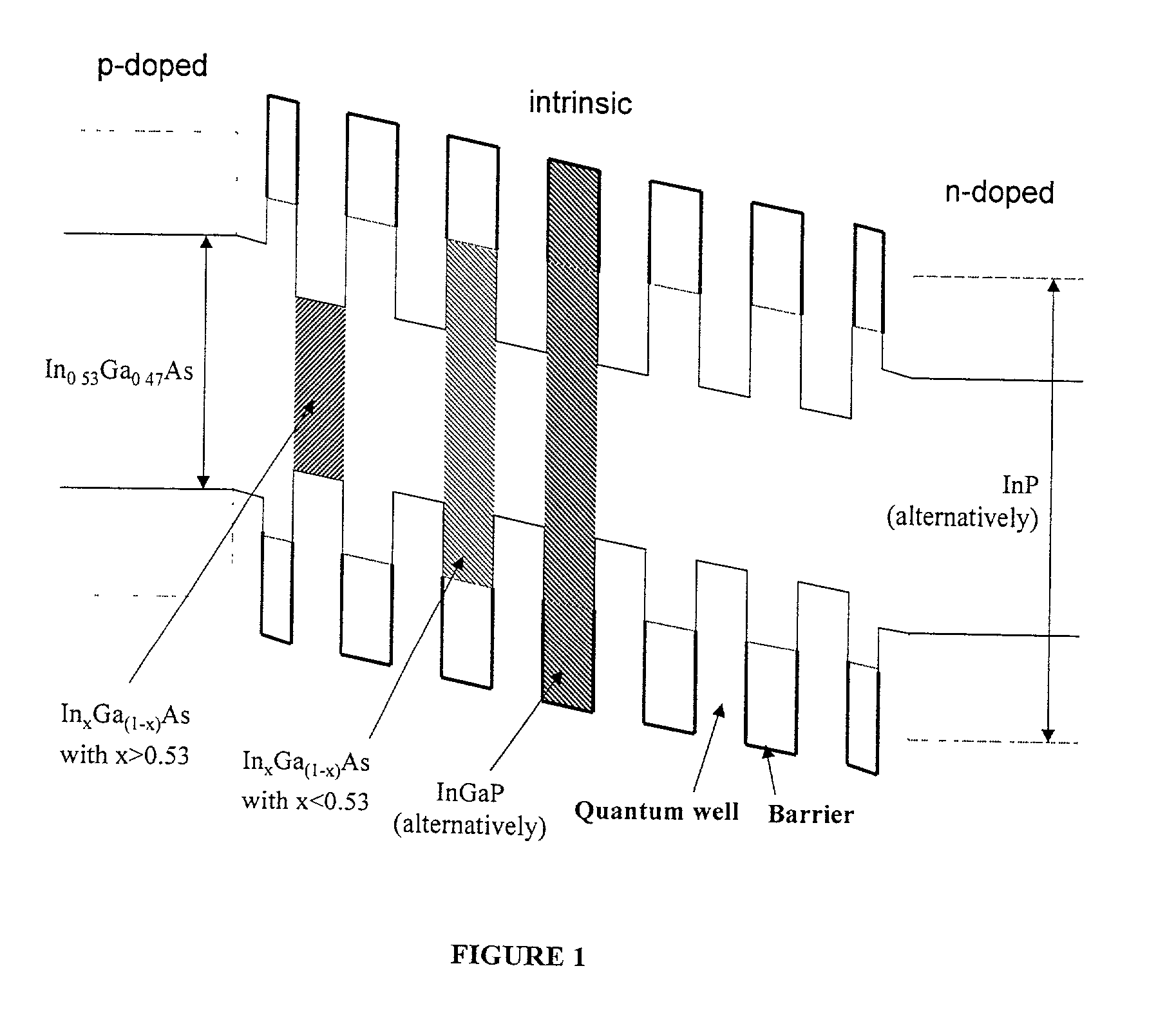
[0026] In FIG. 2 the strain-balancing conditions of one example are shown, where the average lattice-constant of wells and barriers is roughly the same as the InP substrate. FIG. 1 shows a schematic diagram of the energy band-gaps of this kind of structure. This specific sample was not designed for TPV applications; the p-region, for example, is far too thick. It does not quite fulfil the ideal strain-balanced conditions,...


PUM


Abstract

A photovoltaic cell to convert low energy photons is described, consisting of a p-i-n diode with a strain-balanced multi-quantum-well system incorporated in the intrinsic region. The bandgap of the quantum wells is lower than that of the lattice-matched material, while the barriers have a much higher bandgap. Hence the absorption can be extended to longer wavelengths, while maintaining a low dark current as a result of the higher barriers. This leads to greatly improved conversion efficiencies, particularly for low energy photons from low temperature sources. This can be achieved by strain-balancing the quantum wells and barriers, where each individual layer is below the critical thickness and the strain is compensated by quantum wells and barriers being strained in opposite directions minimizing the stress. The absorption can be further extended to longer wavelengths by introducing a strain-relaxed layer (virtual substrate) between the substrate and the active cell.

Description

[0001] 1. Field of the Invention[0002] This invention relates to an improved photovoltaic device / cell for the conversion of heat radiation into electricity.[0003] 2. Description of the Prior Art[0004] Thermophotovoltaics (TPV) is the use of photovoltaic (PV) cells to convert heat radiation, e.g. from the combustion of fossil fuels or biomass, into electricity. The energy spectrum is often reshaped using selective emitters which absorb the heat and re-emit in a narrow band. The re-emitted radiation may be efficiently converted to electric power using a PV cell of appropriate low band-gap. Higher PV cell efficiencies can be achieved by introducing multi-quantum-wells (MQW) into the intrinsic region of a p-i-n diode if the gain in short-circuit current exceeds the loss in open-circuit voltage [K. W. J. Bartham and G. Duggan, J. Appl. Phys. 67, 3490 (1990). K. Barnham et al., Applied Surface Science 113 / 114, 722 (1997). K. Barnham, International Published Patent Application WO-A-93 / 0860...

Claims


Application Information

Patent Timeline
Patent Type & Authority Applications(United States)
IPC IPC(8): H01L31/0352H01L31/04H01L31/075H02S10/30
CPCB82Y20/00H01L31/035236H01L31/0735H02S10/30Y02E10/544Y02E10/548H01L31/075
Inventor ROHR, CARSTENBARNHAM, KEITH W.J.EKINS-DAUKES, NICHOLASCONNOLLY, JAMES P.BALLARD, IAN M.MAZZER, MASSIMO
Owner IMPERIAL INNOVATIONS LTD
Why Eureka
Try Eureka