Selective growth method, and semiconductor light emitting device and fabrication method thereof

a semiconductor light emitting device and growth method technology, applied in the direction of polycrystalline material growth, crystal growth process, chemically reactive gas growth, etc., can solve the problem of high etching rate in a state where no source is supplied, and achieve the effect of reducing the half-value width of the emission wavelength peak, reducing the etching rate, and efficient fabrication

Inactive Publication Date: 2003-07-31
SAMSUNG ELECTRONICS CO LTD
View PDF12 Cites 239 Cited by
  • Summary
  • Abstract
  • Description
  • Claims
  • Application Information

AI Technical Summary

Benefits of technology

[0008] An object of the present invention is to provide a selective growth method capable of solving the problem associated with degradation of characteristics of a semiconductor light emitting device due to a variation in thickness of an active layer of the device.
[0009] Another object of the present invention is to provide a semiconductor light emitting device and a fabrication method, which are capable of improving characteristics of the device, and more specifically, reducing a half-value width of an emission wavelength peak.
[0011] In general, a plane where the growth rate is high is an unstable plane, and therefore, at the plane where the growth rate is high, an etching rate in a state that any source is not supplied becomes high. On the contrary, a plane where the growth rate is low is a stable plane, and therefore, at the plane where the growth rate is low, the etching rate in the state that the source is not supplied becomes low. Accordingly, even if the thickness distribution of a layer becomes non-uniform, the non-uniformity of the thickness distribution of the layer can be corrected by inserting growth interruption for causing etching in a state that the source is not supplied. As a result of growth interruption, the etching rapidly proceeds at a thick portion formed at a high growth rate, whereas the etching slowly proceeds at a thin portion formed at a low growth rate, so that the difference in thickness between the thick potion formed at the high growth rate and the thin portion formed at the low growth rate can be eliminated. Accordingly, it is possible to reduce the non-uniformity of the thickness distribution of a crystal layer.
[0014] For example, in the case of forming a crystal layer on a three-dimensional surface by selective growth, even if the thickness distribution of the crystal layer becomes non-uniform at the time of growth of the crystal layer, the non-uniformity of the thickness distribution of the crystal layer can be corrected by inserting the growth interruption. To be more specific, as a result of growth interruption, an etching rate at a thick portion becomes higher than that at a thin portion, to eliminate the difference in thickness between the thick portion and the thin portion. Accordingly, by adjusting a period of time of the growth interruption so as to control the amount of etching, the non-uniformity of the thickness distribution of the crystal layer can be reduced, to make the thickness of the crystal layer nearly uniform over the whole region thereof.
[0017] According to the semiconductor light emitting device of the present invention, since the active layer formed by selective growth has an uniform thickness distribution and therefore the thickness of the active layer is nearly uniform over the whole region thereof, it is possible to enhance characteristics of the device, and more specifically, reduce a half-value width of an emission wavelength peak.
[0018] According to the method of fabricating the semiconductor light emitting device in accordance with the present invention, it is possible to efficiently fabricate the above-described semiconductor light emitting device having excellent light emission characteristics not by requiring any change of the existing equipment but by slightly changing the ordinary fabrication process.

Problems solved by technology

In general, a plane where the growth rate is high is an unstable plane, and therefore, at the plane where the growth rate is high, an etching rate in a state that any source is not supplied becomes high.

Method used


Image

  • Selective growth method, and semiconductor light emitting device and fabrication method thereof
  • Selective growth method, and semiconductor light emitting device and fabrication method thereof
  • Selective growth method, and semiconductor light emitting device and fabrication method thereof

Examples


Embodiment Construction

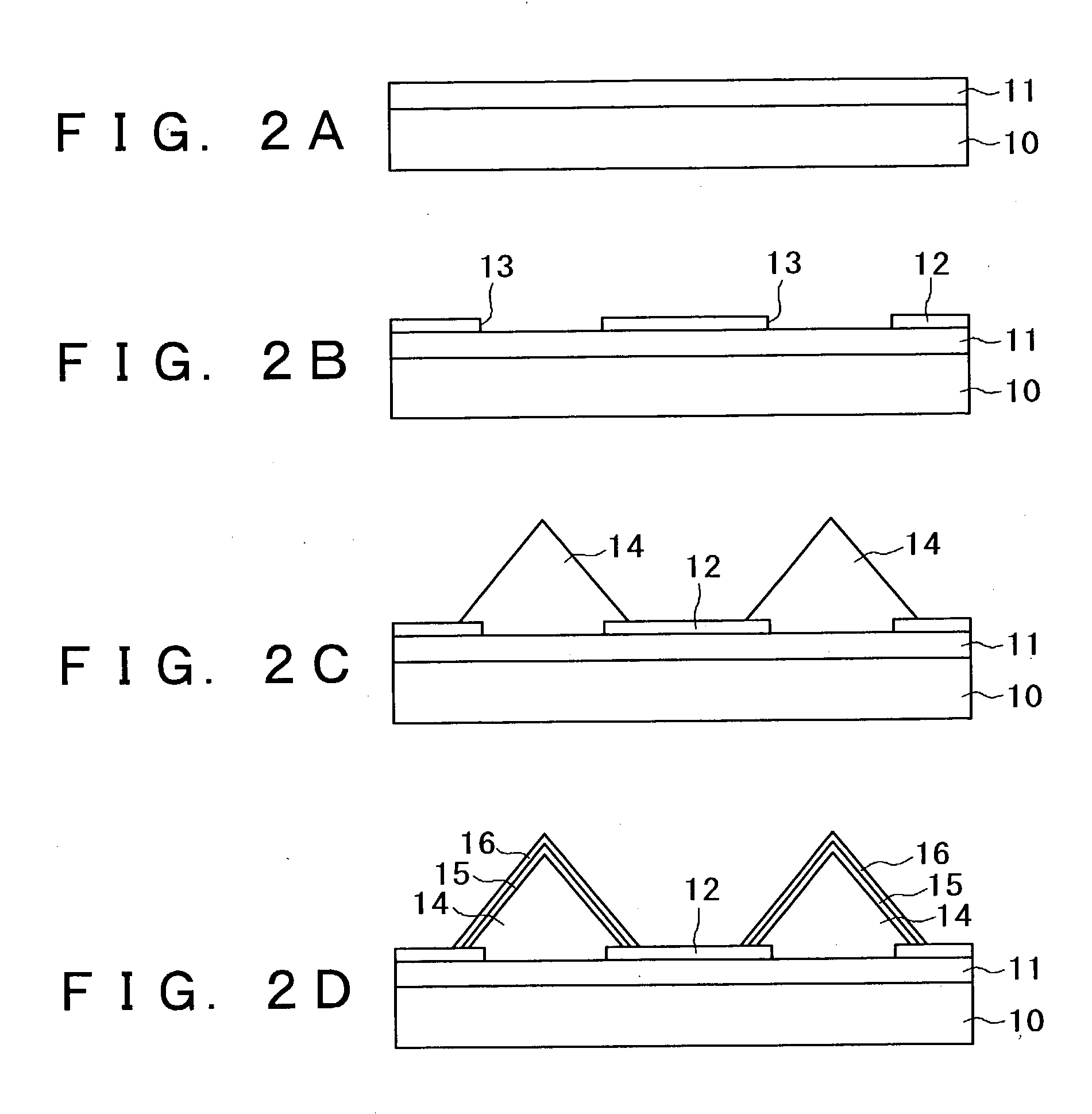
[0029] Hereinafter, a selective growth method, and a semiconductor light emitting device and a fabrication method thereof, to each of which the present invention is applied, will be described in detail with reference to the drawings.

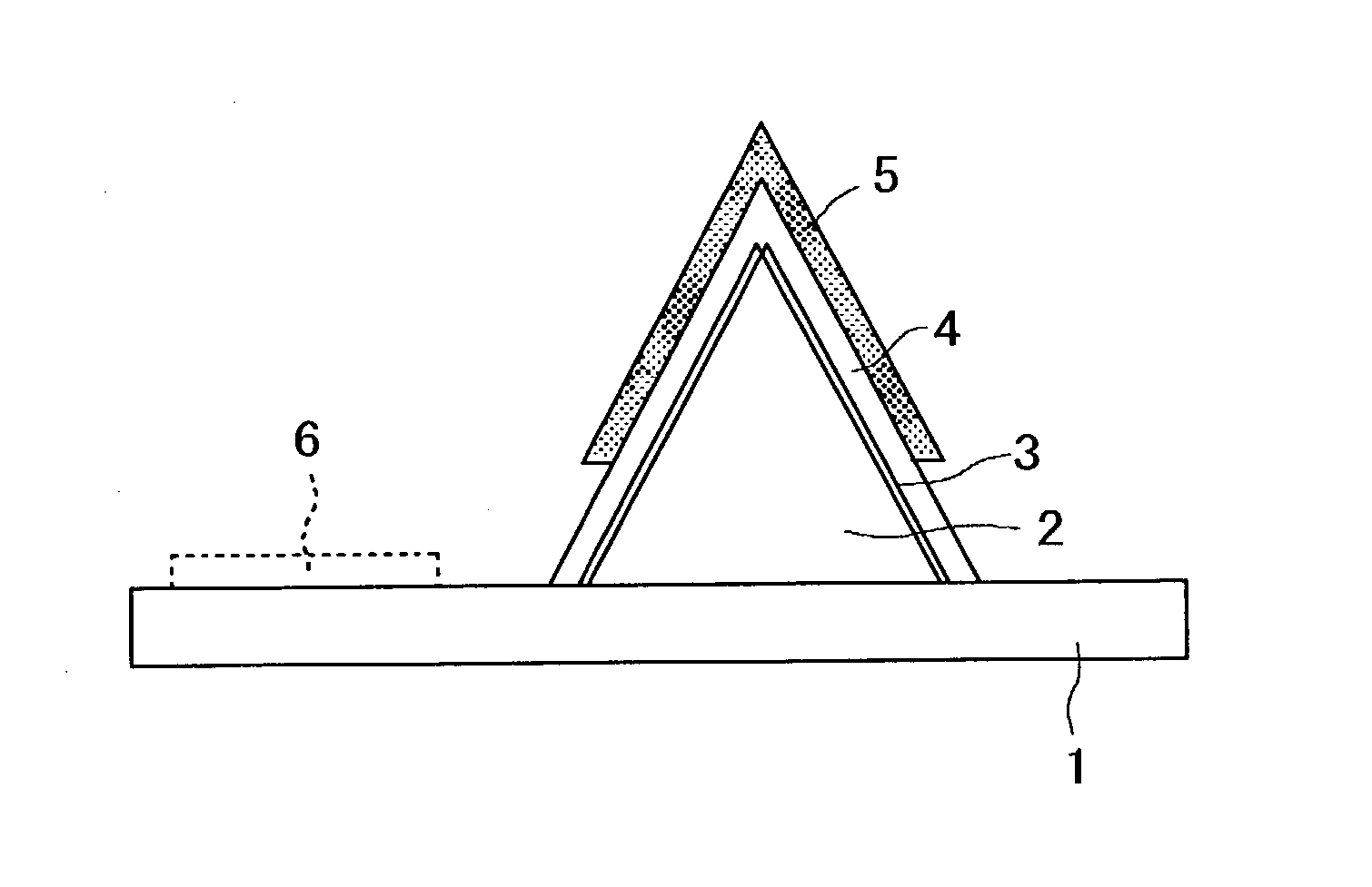
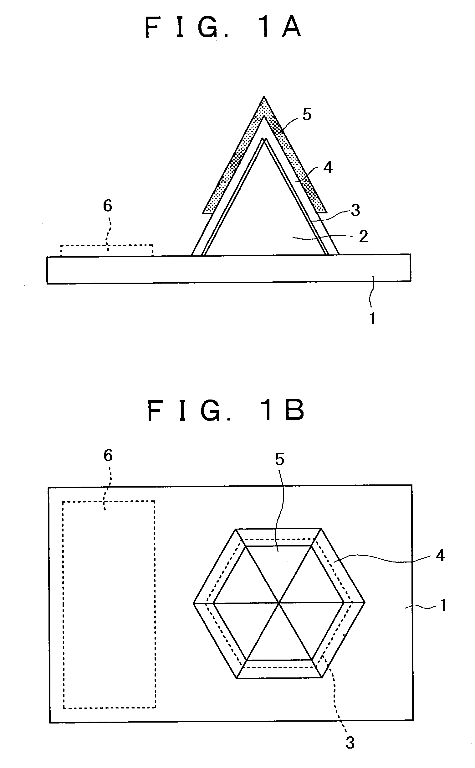
[0030] The selective growth of an active layer according to the present invention will be described by example of a process of fabricating a semiconductor light emitting device having a structure shown in FIGS. 1A and 1B.

[0031] FIGS. 1A and 1B are a sectional view and a plan view showing the structure of a semiconductor light emitting device as one example of a device to which the fabrication process of the present invention is applied, respectively.

[0032] The light emitting device shown in the figures is exemplified by a GaN based light emitting diode, which is formed by crystal growth on, for example, a sapphire substrate. Such a GaN based light emitting diode formed on the sapphire substrate has a feature that it can be easily peeled from the sapphire...


PUM

PropertyMeasurementUnit
temperatureaaaaaaaaaa
angleaaaaaaaaaa
angleaaaaaaaaaa

Abstract

In a selective growth method, growth interruption is performed at the time of selective growth of a crystal layer on a substrate. Even if the thickness distribution of the crystal layer becomes non-uniform at the time of growth of the crystal layer, the non-uniformity of the thickness distribution of the crystal layer can be corrected by inserting the growth interruption. As a result of growth interruption, an etching rate at a thick portion becomes higher than that at a thin portion, to eliminate the difference in thickness between the thick portion and the thin portion, thereby solving the problem associated with degradation of characteristics due to a variation in thickness of the crystal layer, for example, an active layer. The selective growth method is applied to fabrication of a semiconductor light emitting device including an active layer as a crystal layer formed on a crystal layer having a three-dimensional shape by selective growth.

Description

BACKGROUND OF THE INVENTION[0001] The present invention relates to a selective growth method, and to a semiconductor light emitting device and a fabrication method thereof, to each of which the selective growth method is applied.[0002] GaN based compound semiconductors have become a focus of attention as semiconductor materials for semiconductor light emitting devices, and a variety of device designs and trials have been made to improve characteristics of semiconductor light emitting devices using GaN based compound semiconductors.[0003] The GaN based semiconductor light emitting device emits light having a wavelength in a short-wavelength region, and therefore, it allows emission of light of blue or green. Accordingly, a full-color image display unit can be fabricated, for example, by combining the GaN based semiconductor light emitting devices with GaAs based semiconductor light emitting devices allowing emission of light of red.[0004] The above-described GaN based semiconductor l...

Claims


Application Information

Patent Timeline
Patent Type & Authority Applications(United States)
IPC IPC(8): C30B25/02H01L21/20H01L21/205H01L33/06H01L33/16H01L33/32
CPCC30B25/02H01L21/02639C30B29/406H01L33/24H01L21/0237H01L21/0242H01L21/02433H01L21/02458H01L21/02502H01L21/02513H01L21/0254H01L21/02576H01L21/02579H01L21/02587H01L21/02609H01L21/0262C30B29/403
Inventor BIWA, GOSHIOKUYAMA, HIROYUKI
Owner SAMSUNG ELECTRONICS CO LTD
Why Eureka
Try Eureka