Method of growing oxide films

a technology of oxide film and cvd, which is applied in the direction of crystal growth process, polycrystalline material growth, chemically reactive gas growth, etc., can solve the problems of cvd not always achieving a sufficiently good coverage with thin layers, and the component's functional point of view is disadvantageously high,

Inactive Publication Date: 2003-10-09
ASM IP HLDG BV
View PDF29 Cites 295 Cited by
  • Summary
  • Abstract
  • Description
  • Claims
  • Application Information

AI Technical Summary

Benefits of technology

[0014] The invention is based to the discovery that the above mentioned objectives can be achieved by using a silicon compound containing an organic ligand as the silicon source and a reactive oxygen source, such as ozone, as the oxygen source material. Multicomponent oxides in which the amount of silicon dioxide can be varied in a controlled way can easily be prepared by the proposed solution.
[0018] Remarkable advantages are achieved with the aid of the invention. Thus, the ALD process provides a possibility far growing a multistaged interlayer containing both silicon dioxide and metal oxide prior to growing the actual metal oxide, which has a high dielectricity. The stability of the capacitor dielectric can be increased by mixing amorphous silicon dioxide into the dielectric. The preparing of multicomponent oxides and the advantages achieved thereof are described in more detail below.
[0020] In the components needed in magnetic recording silicon dioxide can be used as the isolation layer in both the writing / reading head and in the encapsulation of the writing / reading head. In order to avoid the destruction of the magnetic properties of the layers, that are already built, the processing temperature must be low in all steps. In general, physical (sputtering) methods are used in the field, the problem of said methods being the unevenness of produced film. ALD bas the capability to produce both physically and electrically homogenous thin film. It is especially preferable to use a low temperature ALD silicon dioxide process that provides a uniformly covering and electrically homogenous SiO.sub.2 thin film. In this way the reproducibility and reliability of this process step can be increased.

Problems solved by technology

The continual decrease in the size of microelectronics components is leading into a situation in which SiO.sub.2 can no longer be used as the gate dielectric (gate oxide) of MOSFET (metal-oxide-semiconductor field-effect transistor) since for achieving required capacitances the SiO.sub.2 layer should be made so thin that the tunneling current increases disadvantageously high from the functional point of view of the component.
Materials having sufficiently high dielectric constants are abundant, but the problem is that the considered dielectric should be stable on the silicon surface, should most preferably be amorphous and should endure nearly unchanged under high post-treatment temperatures.
The conventional CVD method is related to the difficulty of controlling the process, and neither a sufficiently good coverage with the thin layers nor a good conformality is always achieved by CVD.
The disadvantages of these known solutions are long reaction times, for what reason the proposed processes cannot be realized on an industrial scale.

Method used


Image

  • Method of growing oxide films
  • Method of growing oxide films
  • Method of growing oxide films

Examples


example 1

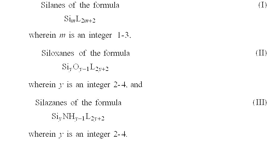
[0045] SiO.sub.2 films were grown in a flow type F-120 ALCVD.TM.reactor (ASM Microchemistry Ltd.). 3-aminopropyltriethoxy silane NH.sub.2-CH.sub.2CH.sub.2CH.sub.2-Si(O-CH.sub.2CH.sub.3).sub.3 (AMTES), 3-aminopropyltrimethoxy silane (NH.sub.2-CH.sub.2CH.sub.2CH.sub.2-Si(O-CH-.sub.3).sub.3 (AMTMS) and hexamethyldisilazane (CH.sub.3).sub.3Si-NH-Si(CH-.sub.3).sub.3 (HMDS) were used as the silicon source material. Ozone (0.sub.3) was used as the oxygen source material. AMTES and AMTMS were inside of the reactor. Ozone and HMDS were led into the reactor from outside. The reaction temperature of AMTES was 200 or 300 .degree.C, that of AMTMS 300 .degree.C and HMDS 400 .degree.C.

[0046] The growing of SiO.sub.2 from AMTES was carried out with the aid of alternating AMTES and ozone pulses between of which the reaction space was purged carefully so that the source materials would not be simultaneously present in the reaction space. The duration of the AMTES pulse was 1,0 s and that of the purgi...

example 2

[0049] Multicomponent oxides were grown in the above reactor using AMTMS as the silicon source material. In the growing processes the AMTMS pulse was 0,5 s, the purging pulse 0,5 s, the ozone pulse 3,5 s and the purging pulse 1 s. The pulse of the metal source material was correspondingly 0,5 s and the purging pulse 0,5 s. If water was used as the oxygen source the duration of the water pulse was 0,2 s and that of the purging pulse 0,5 s. Using ozone with the metal source material the duration of the ozone pulse was 3,5 s and that of the purging pulse 0,5 The growth rates and cycle ratios, are shown in the table below.

2 Multicomponent Metal Source Total Amount of Growth rate Oxide Material Cycles / Cycle ratio (M:S) .ANG. / cycle SiTiOx TiCl.sub.4 1800 / (1:1) 0,9 SiTaOx TaCl.sub.5 1800 / (1:1) 1,1 SiHfOx HfCl.sub.4 700 / (1:1) 1,23 SiZrOx ZrCl.sub.4 700 / (1:1) 1,1 SiZrOx (repeat) ZrCl.sub.4 700 / (1:1) 1,1 SiAlOx Al(CH.sub.3) 1900 / (1:1) 1,0 SiLaOx La(thd).sub.3 1100 / (1:1) 0,75 SiYOx Y(thd).sub....


PUM

PropertyMeasurementUnit
pressureaaaaaaaaaa
boiling pointaaaaaaaaaa
pressureaaaaaaaaaa

Abstract

Abstract of Disclosure Process for producing silicon oxide containing thin films on a growth substrate by the ALCVD method. In the process, a vaporisable silicon compound is bonded to the growth substrate, and the bonded silicon compound is converted to silicon dioxide. The invention comprises using a silicon compound which contains at least one organic ligand and the bonded silicon compound is converted to silicon dioxide by contacting it with a vaporised, reactive oxygen source, in particular with ozone. The present invention provides a controlled process for growing controlling thin films containing SiO2, with sufficiently short reaction times.

Description

Cross Reference to Related Applications[0001] The present application is a U.S. national phase application under 35 U.S.C. .sctn. 371, based on PCT / FI00 / 01072, filed December 4, 2000, and claims priority under 35 U.S.C. .sctn. 119 to Finnish Patent Application Number FI 19992616, filed December 3, 1999.Background of InventionField of the Invention[0002] The present invention relates to a method according to the preamble of Claim 1 of producing oxide films.[0003] According to such a method a thin film containing silicon dioxide is produced on a growth substrate by an ALD method by bonding a vaporisable silicon compound onto the growth substrate and converting the bonded silicon compound to silicon dioxide.[0004] The invention also relates to a method according to the preamble of Claim 20 of producing multicomponent oxides (i.e. mixed oxides or tertiary oxides).Description of the Related Art[0005] The continual decrease in the size of microelectronics components is leading into a situ...

Claims


Application Information

Patent Timeline
Patent Type & Authority Applications(United States)
IPC IPC(8): C23C16/40C23C16/44C23C16/455C30B25/02C23C16/42H01L21/316
CPCC23C16/401C23C16/402H01L21/31612C23C16/44C23C16/45531C30B25/02H01L21/02145H01L21/02148H01L21/0215H01L21/02153H01L21/02156H01L21/02159H01L21/02164H01L21/02211H01L21/02216H01L21/02222H01L21/0228C30B29/16H01L21/203
Inventor TOIS , EVAHAUKKA , SUVITUOMINEN , MARKO
Owner ASM IP HLDG BV
Why Eureka
Try Eureka