Pattern formation process for an integrated circuit substrate

Inactive Publication Date: 2003-10-09
VIA TECH INC
View PDF9 Cites 19 Cited by
  • Summary
  • Abstract
  • Description
  • Claims
  • Application Information

AI Technical Summary

Problems solved by technology

The process described above has been developed for many years in prior art, however, the disadvantages still exist; such as bad reliability, bad yield and so on.
1. The solder mask is the most common used material in filling process fro the PTH 14, it is easy to form the gap space in the conducting plug 15 and to produce the popcorn, and further cause the difficulties of filling, the limitation of the diameter of the via, bad quality of electrical connection and bad reliability.
2. Making hi

Method used


Image

  • Pattern formation process for an integrated circuit substrate
  • Pattern formation process for an integrated circuit substrate
  • Pattern formation process for an integrated circuit substrate

Examples


first embodiment

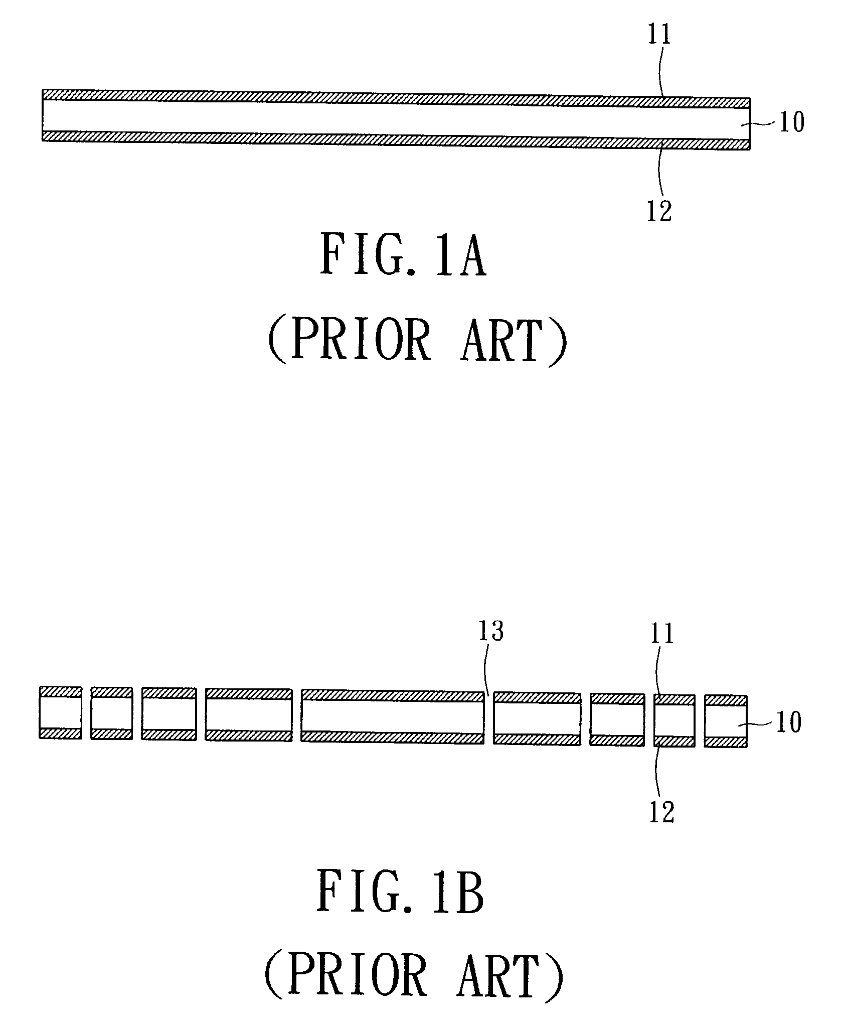
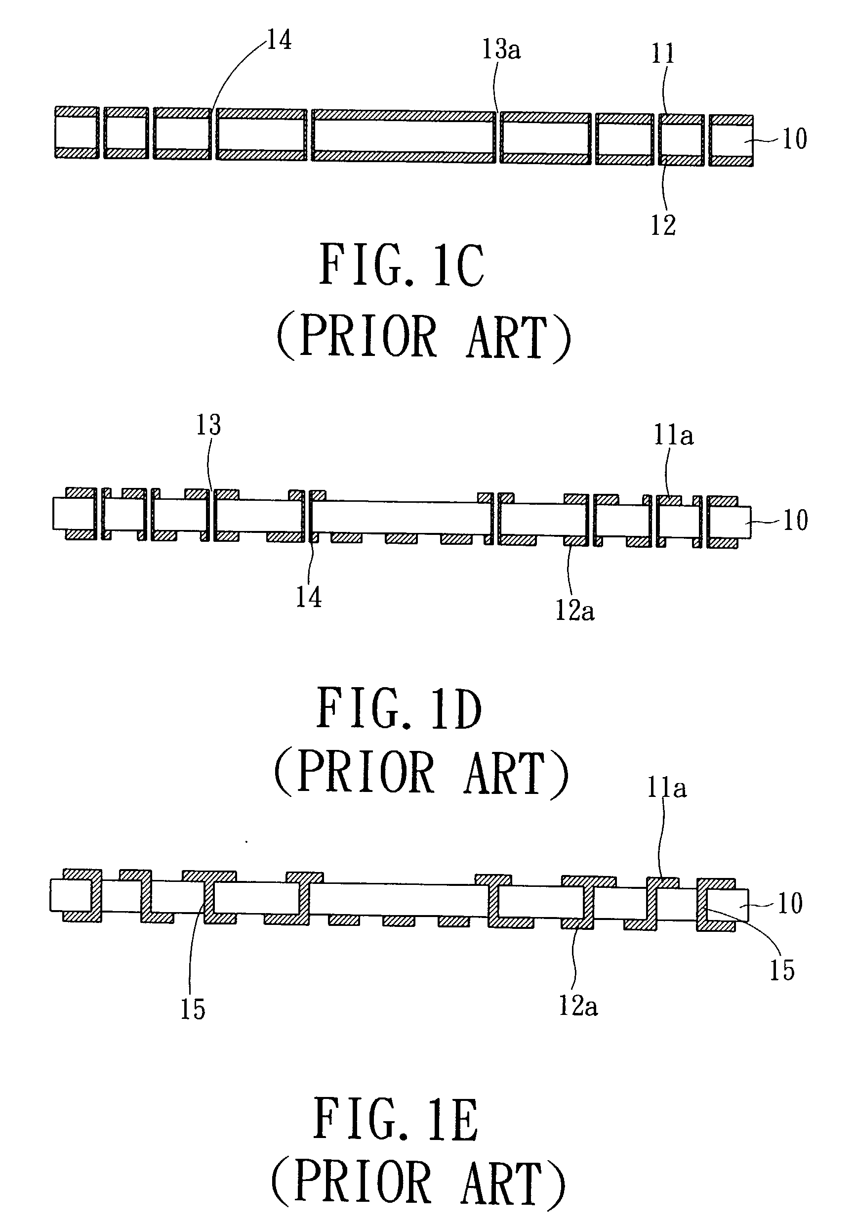
[0034] Please refer to FIG. 2A to FIG. 2M, which are showing the pattern formation process for an integrated circuit substrate of the present invention. The steps of forming the pattern and filling the via with conductive material are as follows:

[0035] (a) selecting a substrate 110 which can be a ceramic substrate, a plastic substrate or a soft material substrate. The ceramic substrate uses the ceramic material as isolation while the plastic substrate uses the plastic material as isolation. And the plastic substrate is the common one adapted in the industry, generally, the material for the plastic substrate is epoxy resin FR-4, BMI, BT-based resin, teflon, LCP, or polyimide. Then, a protection sheet 111 will be placed on the surface of the substrate 110, and on the predetermined position of the substrate 110, a few through hole structure 13a penetrating through the substrate 110 will be made by the mechanical drilling or the laser process.

[0036] (b).placing a protection release shee...

second embodiment

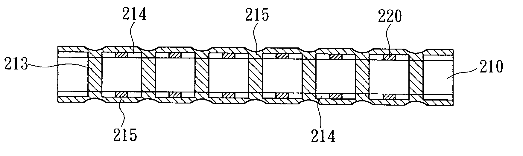
[0049] Please refer to FIG. 3A to FIG. 3K, which are showing the pattern formation process for an integrated circuit substrate of the present invention. The steps of manufacturing the via and filling the via with conductive material are as follows:

[0050] (a) selecting a substrate 210 which can be a ceramic substrate, a plastic substrate or a soft material substrate. The ceramic substrate uses the ceramic material as isolation while the plastic substrate uses the plastic material as isolation. Then, a protection sheet 211 will be placed on the surface (top one) of the substrate 210, and on the predetermined position of the substrate 210, a few through hole structure 213a penetrating through the substrate 210 will be made by the mechanical drilling or the laser process.

[0051] (b).placing a protection release sheet 212 on the other surface (the bottom one) of the circuit substrate 210 that has not been placed with a protection sheet 211, and applying one of the metal spray method, meta...


PUM

PropertyMeasurementUnit
Electrical conductoraaaaaaaaaa
Velocityaaaaaaaaaa

Abstract

A pattern formation process for an integrated circuit substrate, which is not employing the conventional method of filling resin material directly in via filling process but adapting the metal spray method, the metal vapor deposition method or any combination thereof to form the pattern including circuits and pads and stuff the vias and the through holes.

Description

[0001] (a) Field of the invention[0002] The present invention relates to a pattern formation process for an integrated circuit substrate. Especially, the present invention relates to a pattern formation process that uses the metal spray method, the metal vapor deposition method or any combination thereof applying on the integrated circuit substrate to stuff the vias and PTHs ((Plated Through Holes) and to form the pattern including circuits and pads.[0003] (b) Description of the Prior Art[0004] As the electronic product getting smaller and lighter, the circuit board and the substrate manufacturer now are facing the strict requirement for multiple layers integrated circuit substrate. The circuit layout placed on the substrate is using the vias and the PTHs to connect and conduct each other. Basically, the PTH is fully penetrating through a substrate, while a via is not when several substrates added together. In general, the diameter of the via or the PTH is less than 100 .mu.m and it...

Claims


Application Information

Patent Timeline
IPC IPC(8): C23C4/18H05K3/40H05K3/46
CPCC23C4/185H05K3/467H05K3/4076
Inventor KUNG, MORISSHO, KWUN-YAO
Owner VIA TECH INC
Why Eureka
Try Eureka