

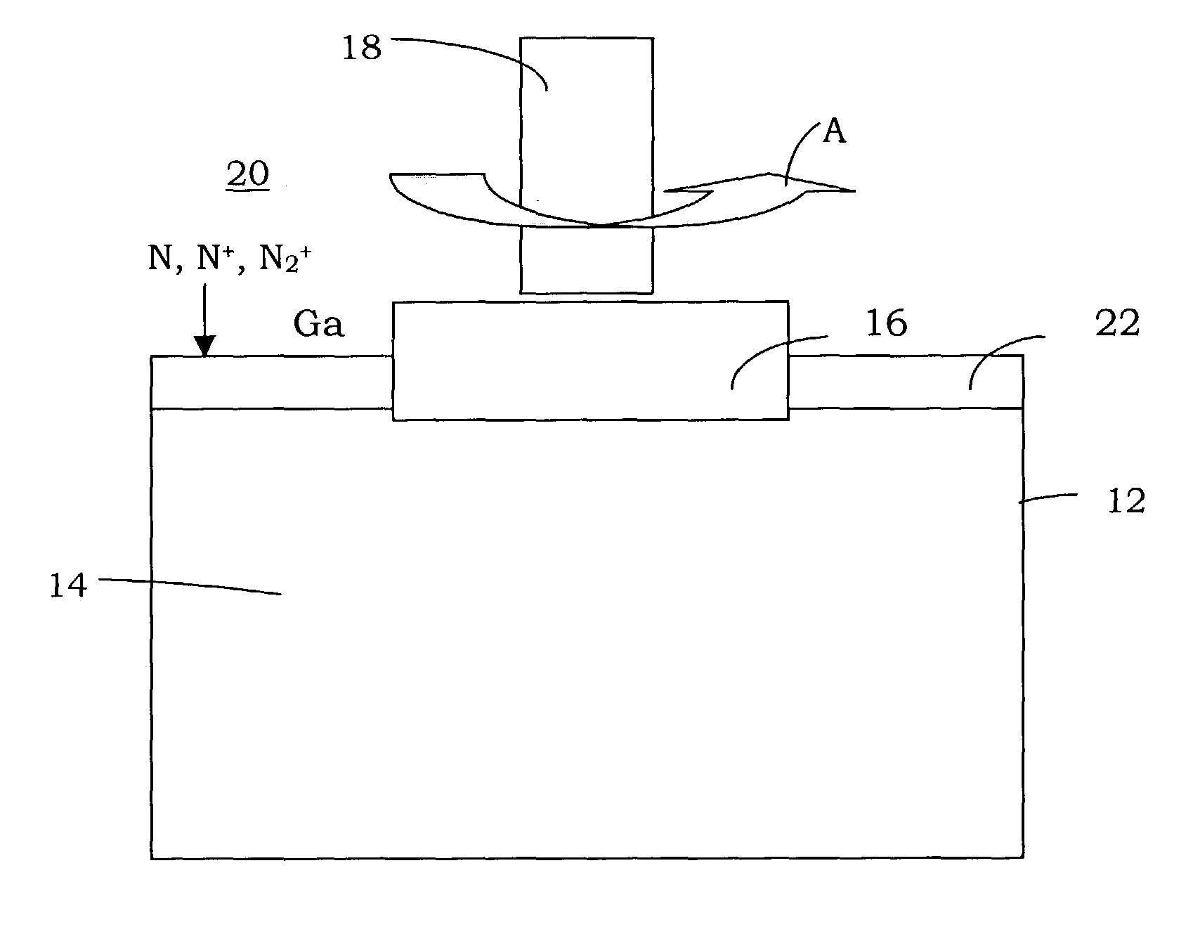
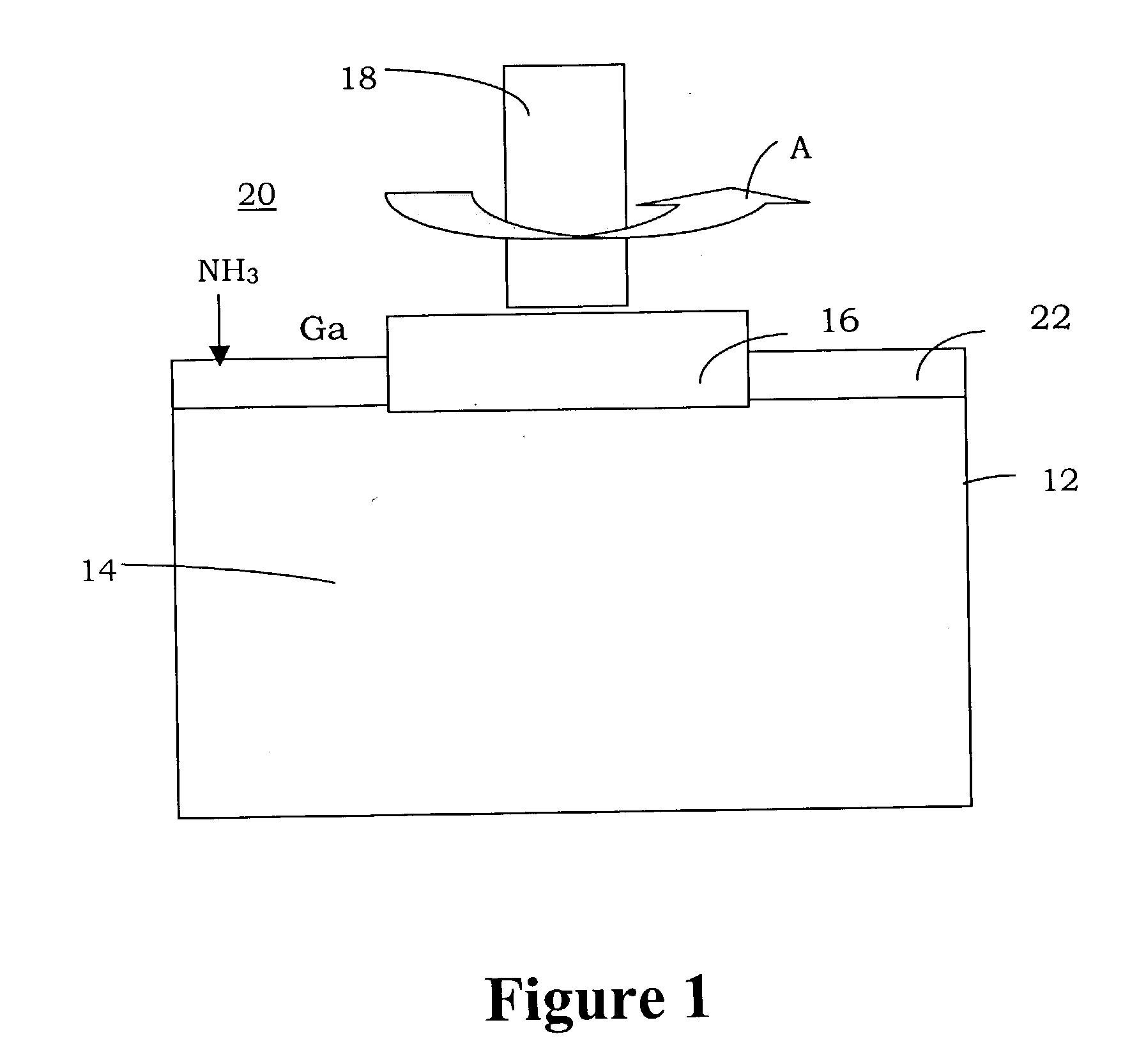
GaN boule grown from liquid melt using GaN seed wafers
a technology of gan boule and liquid melt, which is applied in the direction of crystal growth process, polycrystalline material growth, and growth of polycrystalline materials under a protective fluid, can solve the problems of limited realization of full potential, inability to grow bulk crystals of nitrides with conventional methods, and inability to meet the requirements of electronic and optoelectronic applications,
- Summary
- Abstract
- Description
- Claims
- Application Information
AI Technical Summary
Problems solved by technology
Method used
Image

Examples
Embodiment Construction
[0074] The disclosures of the following United States Patents and United States Patent Applications, collectively referred to hereinafter as "Bulk GaN Technology References," are hereby incorporated herein by reference in their respective entireties:
[0075] U.S. patent application Ser. No. 08 / 188,469 filed Jan. 27, 1994 in the names of Michael A. Tischler, et al., now issued as U.S. Pat. No. 5,679,152;
[0076] U.S. patent application Ser. No. 08 / 955,168 filed Oct. 21, 1997 in the names of Michael A. Tischler, et al.;
[0077] U.S. patent application Ser. No. 08 / 984,473 filed Dec. 3, 1997 in the names of Robert P. Vaudo, et al., now issued as U.S. Pat. No. 6,156,581;
[0078] U.S. patent application Ser. No. 09 / 179,049 filed Oct. 26, 1998 in the names of Robert P. Vaudo, et al.;
[0079] U.S. patent application Ser. No. 09 / 524,062 filed Mar. 13, 2000 in the names of Robert P. Vaudo, et al.;
[0080] U.S. patent application Ser. No. 09 / 605,195 filed Jun. 28, 2000 in the names of Jeffrey S. Flynn, et...
PUM
| Property | Measurement | Unit |
|---|---|---|
| diameter | aaaaa | aaaaa |
| melt temperature | aaaaa | aaaaa |
| melt temperature | aaaaa | aaaaa |
Abstract
Description
Claims
Application Information