

Biosensor
- Summary
- Abstract
- Description
- Claims
- Application Information
AI Technical Summary
Benefits of technology
Problems solved by technology
Method used
Image

Examples
embodiment 1
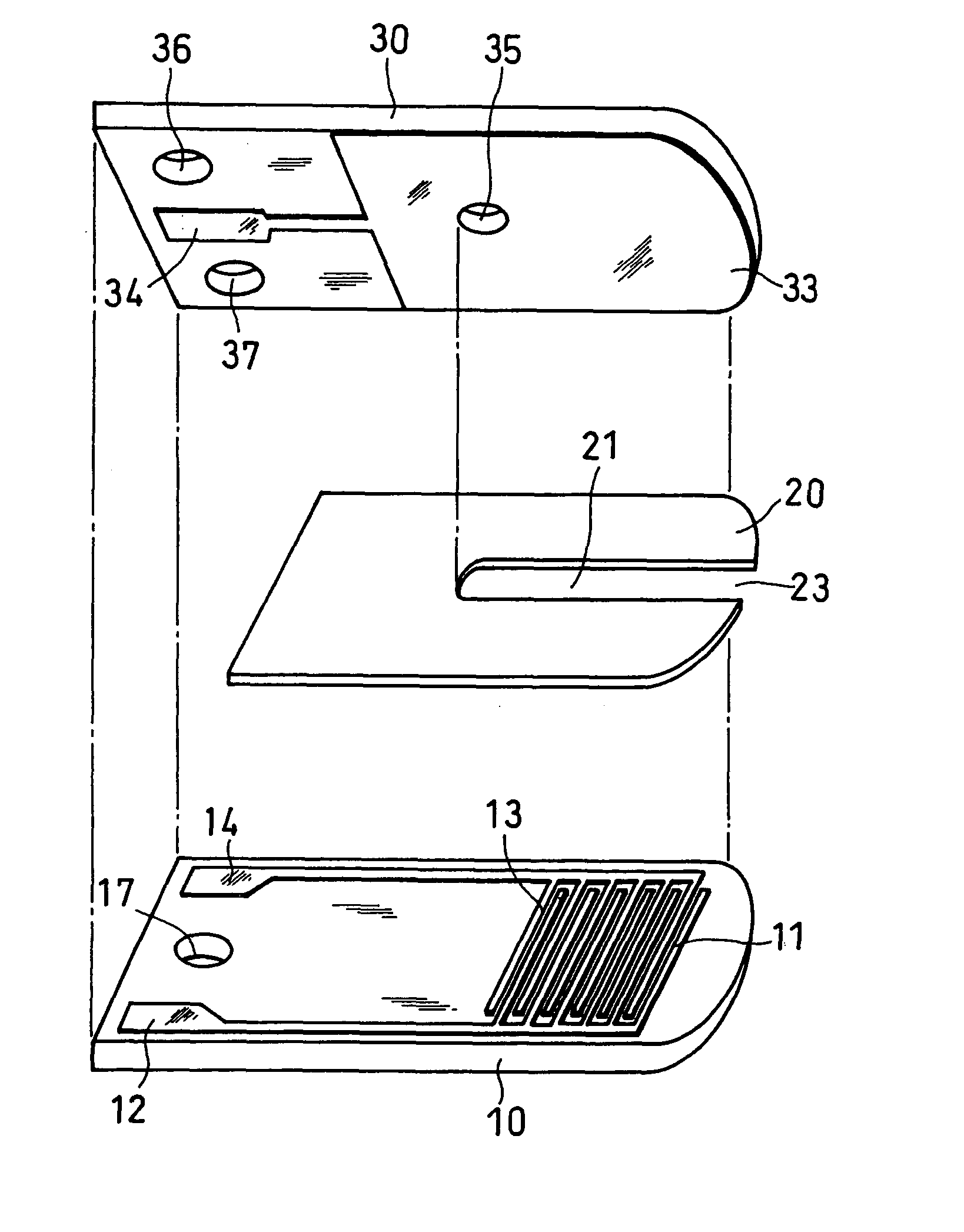
[0059] A glucose sensor having the structure as illustrated in produced. In this example, each of the working electrode 11 and the first counter electrode 13 was a comb-shaped electrode having 65 branches at intervals of 15 .mu.m, each branch being 5 .mu.m in width, and the working electrode branches and the counter electrode branches were arranged alternately at intervals of 5 .mu.m.
[0060] The reagent layer was formed by dropping an aqueous solution containing GOD and potassium ferricyanide onto the electrode system of the first base plate 1 and drying it. Further, a surfactant layer containing lecithin as a surfactant was formed on the reagent layer.
[0061] Thereafter, using solutions containing certain amounts of glucose as samples, glucose concentrations were measured. In this example, the first counter electrode 13 and the second counter electrode 33 were short-circuited to make them function as a counter electrode. A sample was supplied to the sample supply pathway from the sam...
example 2
[0064] A glucose sensor having the structure as illustrated in Embodiment 2 was produced. In this example, each of the first working electrode 41 and the second counter electrode 63 was a comb-shaped electrode having 32 branches at intervals of 15 .mu.m, each branch being 5 .mu.m in width, and each of the second working electrode 61 and the first counter electrode 43 was a comb-shaped electrode having 33 branches at intervals of 15 .mu.m, each branch being 5 .mu.m in width. The first working electrode branches and the first counter electrode branches were arranged alternately at intervals of 5 .mu.m, and the second working electrode branches and the second counter electrode branches were arranged alternately at intervals of 5 .mu.m. Then, the sensor was fabricated such that the first working electrode was opposed to the second counter electrode and the second working electrode was opposed to the first counter electrode. The reagent layer and the surfactant layer have the same struct...
example 3
[0066] A sensor which was the same as that of Example 1 except for the addition of the reference electrode 15 as illustrated in FIG. 6 was produced. The sensor was set to a measuring apparatus as illustrated in FIG. 9, and a sample was supplied to the sample supply pathway from the sample supply inlet 23. 25 seconds after the supply of the sample, a voltage of 300 mV was applied to the working electrode 11 with respect to the reference electrode 15. 5 seconds after the voltage application, the value of the current flowing between the working electrode 11 and the counter electrode was measured, and the measured current value was converted into a voltage value by the current / voltage conversion circuit 78.
[0067] The sensor of Example 3 yielded highly sensitive response similarly to the sensor of Example 1. Further, since it had the reference electrode, the potential of the working electrode could be stabilized in comparison with the two-electrode system and the variation in response va...
PUM
 Abstract
Description
Claims
Application Information