Buffer circuit, buffer tree, and semiconductor device
a buffer circuit and buffer technology, applied in the direction of logic circuit coupling/interface arrangement, pulse manipulation, pulse technique, etc., to achieve the effect of reducing delay time and sufficient setup and hold times
- Summary
- Abstract
- Description
- Claims
- Application Information
AI Technical Summary
Benefits of technology
Problems solved by technology
Method used
Image

Examples
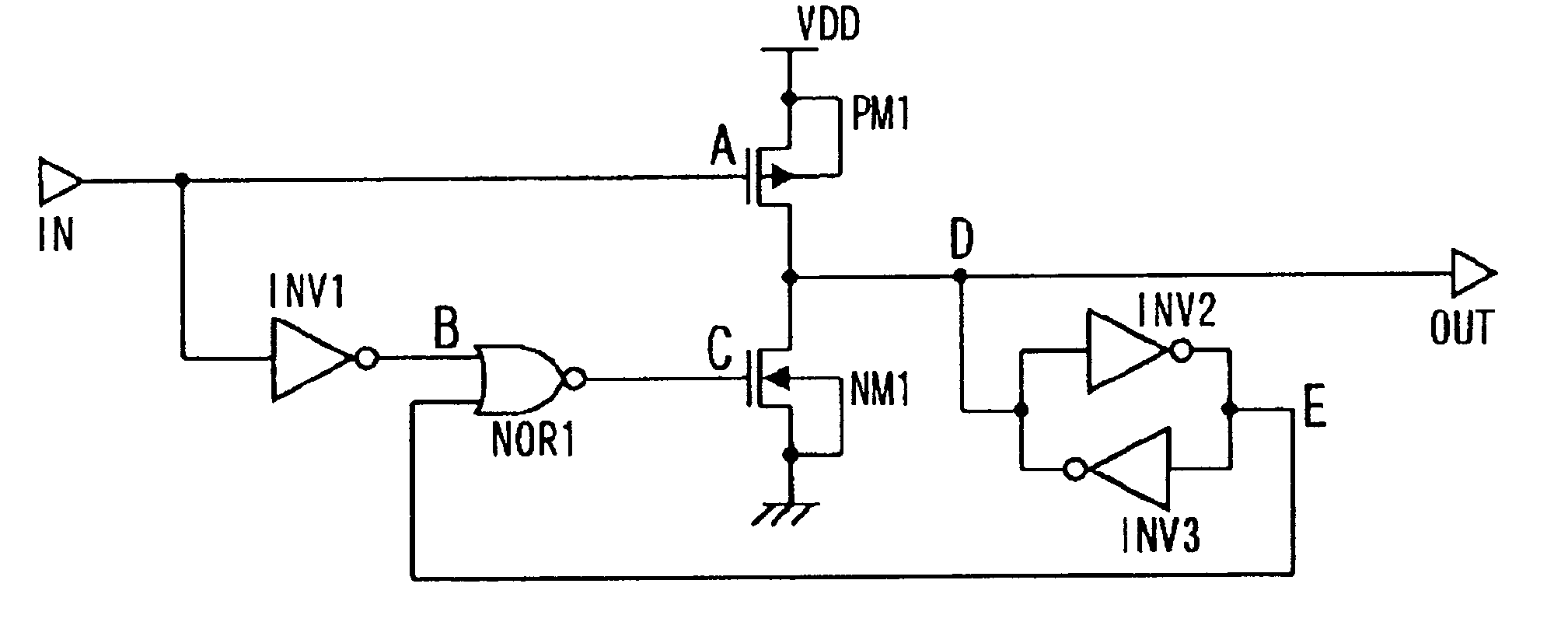
first embodiment
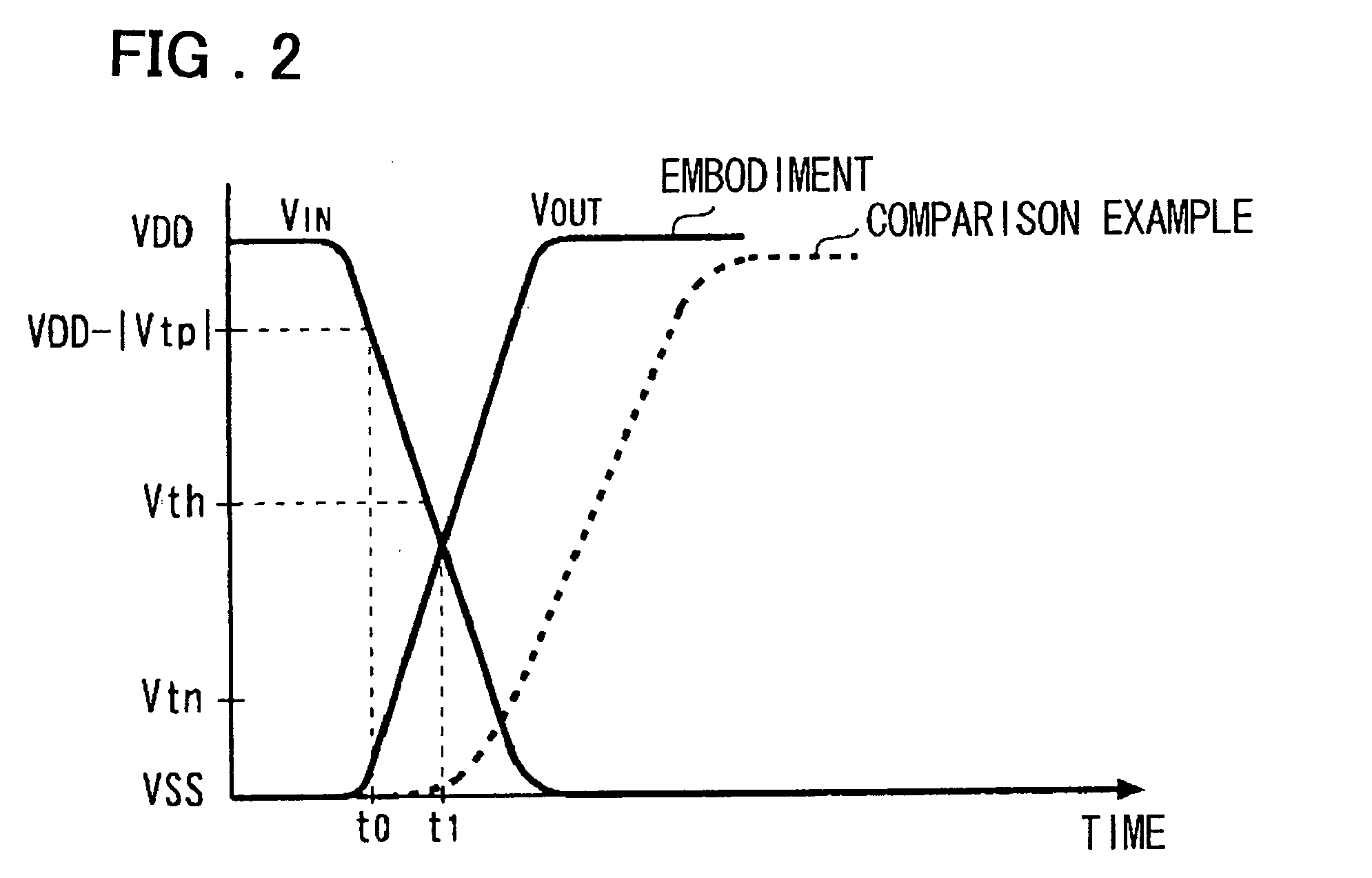
[0068] FIG. 2 is a waveform diagram showing an operation of the present invention. Referring to FIG. 2, at a time point (t0) when an input signal voltage VIN of the input terminal IN has become equal to or lower than VDD-.vertline.Vtp.vertline., where the Vtp is the threshold voltage of the PMOS transistor PM1, an output signal voltage VOUT of the output terminal OUT begins to rise.
[0069] On contrast therewith, in a CMOS inverter (for a comparison example), composed of a PMOS transistor and an NMOS transistor connected in series between the power supplies VDD and VSS, which commonly receive the input signal at their gates and in which a connection point between their drains is connected to the output terminal, when the input signal voltage VIN undergoes a transition to be equal to or lower than VDD-.vertline.Vtp.vertline., the PMOS transistor is turned on and the NMOS transistor, however, is also in an on state. Accordingly, the short-circuit current flows from the power supply VDD ...
second embodiment
[0085] FIG. 7 is a chart for explaining an operation of the present invention shown in FIG. 5. Referring to FIG. 7, IN denotes a signal waveform at the input terminal, A denotes the signal waveform at a node for the gate of the NMOS transistor NM1, B denotes a signal waveform at the node for the output of the inverter INV1 (first input to the NAND1), C denotes a signal waveform at the node for the gate of the PMOS transistor PM1, D denotes a signal waveform at the node for the connection point between drains of the PMOS transistor PM1 and the NMOS transistor NM1, and E denotes a signal waveform at the node for the output of the inverter INV2 (second input to the NAND1), in FIG. 5.
[0086] When the input signal rises at the timing To in FIG. 7, the NMOS transistor NM1 is turned on to make the output terminal OUT (node D) low. At this time, the output node E of the inverter INV2 is at a high level.
[0087] When the input signal supplied to the input terminal (IN) of the buffer circuit fal...
fourth embodiment
[0097] FIG. 10 is a timing chart showing an operation of the present invention. In this embodiment, when the input signal fed to the input terminal IN rises from a low level to a high level (at T.sub.0), the node B which is an output node of the inverter INV1 goes to a low level, in response to the transition of the input signal. At this time, because the output signal of the delay circuit 100 is still at a low level (a high-level signal is not outputted to the node E), the NOR circuit NOR1, which receives a low level at the node E, changes the output node C to a high level, in response to the transition of the node B to the low level. When the node C goes to a high level, the NMOS transistor NM1 is turned on, so that the output terminal OUT goes to a low level.
[0098] The delay circuit 100 that receives the input signal from the input terminal IN delays a rise of the input signal by a time td1, and outputs the delayed signal to the node E, which is the output terminal of the delay c...
PUM
 Abstract
Description
Claims
Application Information
 - R&D
- Intellectual Property
- Life Sciences
- Materials
- Tech Scout
- Unparalleled Data Quality
- Higher Quality Content
- 60% Fewer Hallucinations
Browse by: Latest US Patents, China's latest patents, Technical Efficacy Thesaurus, Application Domain, Technology Topic, Popular Technical Reports.
© 2025 PatSnap. All rights reserved.Legal|Privacy policy|Modern Slavery Act Transparency Statement|Sitemap|About US| Contact US: help@patsnap.com