Semiconductor acceleration sensor using doped semiconductor layer as wiring

a semiconductor layer and acceleration sensor technology, applied in the direction of acceleration measurement in multiple dimensions, acceleration measurement using interia forces, instruments, etc., can solve the problems of reducing the operational reliability of the acceleration sensor, increasing the fluctuation width of the offset voltage, and deteriorating the detection accuracy of the acceleration sensor

Inactive Publication Date: 2004-01-29
MATSUSHITA ELECTRIC WORKS LTD
View PDF7 Cites 21 Cited by
  • Summary
  • Abstract
  • Description
  • Claims
  • Application Information

AI Technical Summary

Problems solved by technology

Thus, there is a problem that the formation of the metal layer 17 on the beam 13' leads to a deterioration of the detection accuracy of the acceleration sensor.
In this case, as a temperature dependency of an offset voltage (i.e., a voltage output from the sensor in an acceleration free state) of the bridge circuit increases, operational reliability of the acceleration sensor lowers.
However, when the wiring for making the electrical connection between the resistor element R and the pad 16 is provided by the metal layer 17, there is another problem that a fluctuation width of the offset voltage increases due to thermal hysteresis.

Method used


Image

  • Semiconductor acceleration sensor using doped semiconductor layer as wiring
  • Semiconductor acceleration sensor using doped semiconductor layer as wiring
  • Semiconductor acceleration sensor using doped semiconductor layer as wiring

Examples


first embodiment

[0037] (First Embodiment)

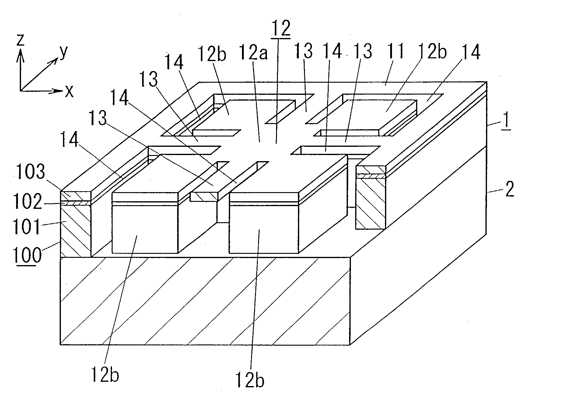
[0038] In a semiconductor multi-axial acceleration sensor of this embodiment, as shown in FIG. 1, a sensor body 1 is formed by use of a SOI substrate 100 having an embedded oxide layer 102 such as silicon oxide as an intermediate layer, and fixed to a glass cover 2 by anodic bonding. The SOI substrate 100 is composed of a base substrate 101 of silicon, an n-type silicon layer (silicon active layer) 103 having a smaller thickness than the base substrate, and the embedded oxide layer 102 provided therebetween as an insulating layer. It is preferred that a thickness of the base substrate 101 is in a range of 400 to 600 .mu.m, thickness of the embedded oxide film 102 is in a range of 0.3 to 1.5 .mu.m, and the thickness of the silicon layer 103 is in a range of 4 to 6 .mu.m.

[0039] As shown in FIGS. 1 and 3, this sensor body 1 has a rectangular frame 11, a weight 12, and two pairs of beams 13 each having a smaller thickness than the frame. The weight 12 is support...

second embodiment

[0068] (Second Embodiment)

[0069] A semiconductor multi-axial acceleration sensor of this embodiment is substantially the same as that of the first embodiment except for the following features. Therefore, no duplicate explanation is deemed to be necessary.

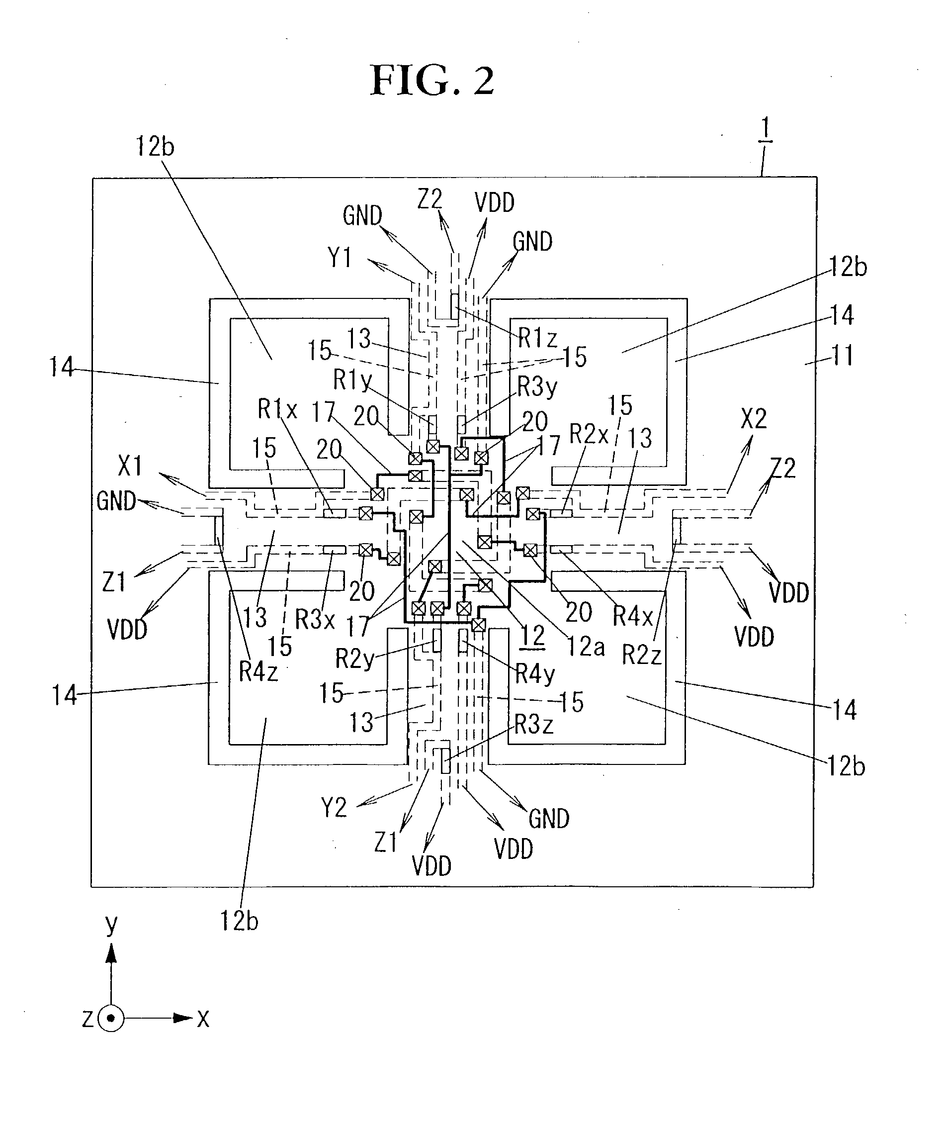
[0070] The acceleration sensor of this embodiment has a wiring layout different from the first embodiment. That is, as shown in FIG. 9, with respect to pair of beams 13 extending in the X-axis direction, wiring patterns of doped semiconductor layers 15 formed on one of the beams 13 and the wiring patterns of the doped semiconductor layers 15 formed on the other beam 13 are symmetric with respect to a vertical center line extending in the Y-axis direction through a center of width of each of the beams. Similarly, with respect to pair of beams 13 extending in the Y-axis direction, wiring patterns of doped semiconductor layers 15 formed on one of the beams 13 and the wiring patterns of the doped semiconductor layers 15 formed on the ot...

third embodiment

[0072] (Third Embodiment)

[0073] A semiconductor multi-axial acceleration sensor of this embodiment is substantially the same as that of the second embodiment except for the following features. Therefore, no duplicate explanation is deemed to be necessary.

[0074] The acceleration sensor of this embodiment has a wiring layout different from the second embodiment. That is, as shown in FIG. 10, with respect to pair of beams 13 extending in the X-axis direction, wiring patterns of doped semiconductor layers 15 formed on one of the beams 13 and the wiring patterns of the doped semiconductor layers 15 formed on the other beam 13 are rotationally symmetric with respect to a center point of the top surface of the center weight 12a by 180 degrees. Similarly, with respect to pair of beams 13 extending in the Y-axis direction, wiring patterns of doped semiconductor layers 15 formed on one of the beams 13 and the wiring patterns of the doped semiconductor layers 15 formed on the other beam 13 are...


PUM


Abstract

A semiconductor acceleration sensor is provided, which has the capability of preventing a situation that detection accuracy of acceleration deteriorates due to undesirable thermal stress induced when a metal layer wiring is used in the acceleration sensor. This sensor comprises a frame, a weight, at least one pair of beams made of a semiconductor material, via which said weight is supported in the frame, and at least one resistor element formed on each of the beams to thereby detect acceleration according to piezoelectric effect of the resistor element. The sensor also includes a doped semiconductor layer formed in a top surface of each of the beams as a wiring for electrically connecting with the resistor element.

Description

[0001] 1. Field of the Invention[0002] The present invention relates to a semiconductor acceleration sensor using piezoelectric effects, and particularly a semiconductor multi-axial acceleration sensor using a doped semiconductor layer as wiring for accurately detecting acceleration in plural directions, which are preferably used for automobiles, home electric appliances, and so on.[0003] 2. Disclosure of the Prior Art[0004] In the past, a piezoelectric-type or a capacitance-type semiconductor acceleration sensor has been widely used in various applications of automobiles, home electric appliances, and so on. As the piezoelectric-type semiconductor acceleration sensor, for example, Japanese Patent Early Publication No. 11-160348 discloses semiconductor multi-axial acceleration sensor for detecting acceleration in plural directions.[0005] As shown in FIG. 16, this sensor is formed with a sensor body 1' having a frame 11', a weight 12' and two pairs of beams 13', via which the weight ...

Claims


Application Information

Patent Timeline
Patent Type & Authority Applications(United States)
IPC IPC(8): G01P15/08G01P15/12G01P15/18
CPCG01P15/0802G01P15/18G01P15/123G01P2015/084G01P2015/0842G01P15/12
Inventor YOSHIDA, HITOSHIKATAOKA, KAZUSHIWAKABAYASHI, DAISUKEGOTO, KOJI
Owner MATSUSHITA ELECTRIC WORKS LTD
Why Eureka
Try Eureka