

Electron beam apparatus and image forming apparatus
a technology of electron beam and image forming apparatus, which is applied in the direction of discharge tube/lamp details, discharge tube/lamp details, discharge tube with screen, etc., can solve the problems of difficult substrate heat melting and inability to faithfully express the position
- Summary
- Abstract
- Description
- Claims
- Application Information
AI Technical Summary
Benefits of technology
Problems solved by technology
Method used
Image

Examples
first embodiment
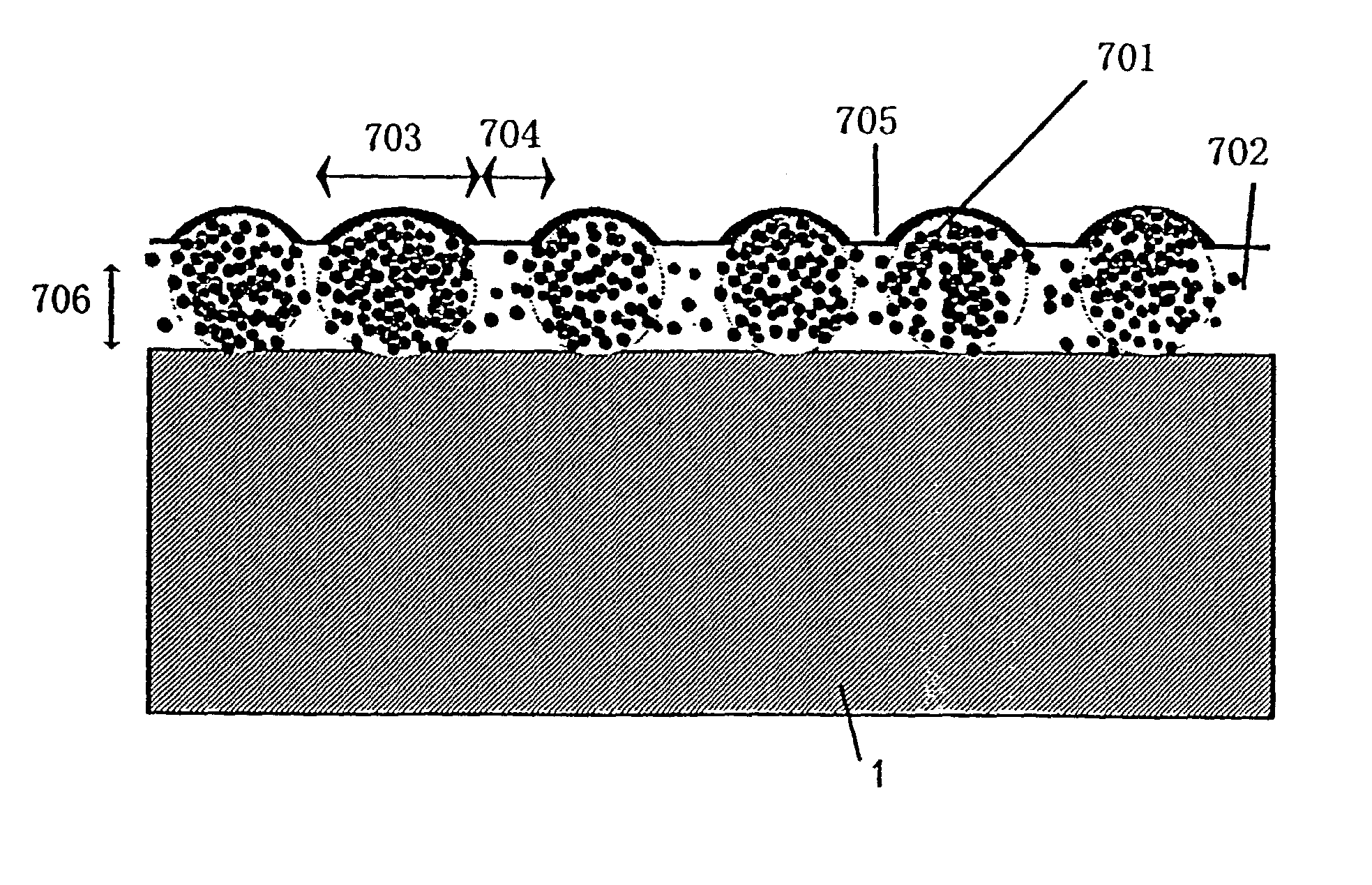
[0160] Hereinafter, in any of the embodiment modes, the average particle diameter of the primary particles (fine particles) is preferable, and as an embodiment mode which particularly suitably roughs the surface, a structure in which the particle diameter of the primary particles is larger than the film thickness is exemplified as a first embodiment mode in FIGS. 6 and 8. In the figures, reference numeral 601 and 801 denote fine particles provided for roughing the surface, and 602 and 802 are binder matrix portions provided for the purpose of fixing the fine particles with respect to the substrate, etc. The fine particle diameters 603 and 803 respectively are so designed as to have large values with respect to the film thicknesses 604 and 804 of the binder matrix portion. From the viewpoints of the substrate adhesion and the electrically conductivity, as shown in FIG. 8, fine particles 806 of another size may be contained in the binder other than the surface roughing fine particles....
second embodiment
[0169] In a second embodiment mode of this embodiment, the thickness of the surface roughing layer which is a layer containing the fine particles is a value larger than the particle diameter of the primary particles and is substantially equal to or smaller than the secondary particles. In this example, the thickness of the surface roughing layer means the average thickness of a region which satisfies the requirements of the present invention.
[0170] The primary particles dispersed in a coating solution form the secondary particles aggregated in a more stable state from a monodisperse state due to unstable factors such as an energy balance of a solid and a solution, a temperature during retention, a light stimulus, an atmosphere during formation of a film and cleaning conditions, thereby being capable of forming the sparse and crowded distribution of the primary particles in the film. In this situation, since the specific resistance of the fine particles in respect to the binder mater...
embodiment 1
[0323] [Embodiment 1]
[0324] A spacer used in this embodiment was produced as follows:
[0325] A ceramic substrate into which zirconia and alumina were mixed with each other at the weight ratio of 65:35 so as to provide the same coefficient of thermal expansion as that of the soda lime glass substrate which was the same in quality as the rear plate was subjected to a grinding process so that its outer dimensions became 0.2 mm in thickness, 3 mm in height and 40 mm in length. The average value of the roughness of the surface was 100 [.ANG.]. The substrate will be referred to as a0.
[0326] First, prior to a film forming process, after the above spacer substrate a0 was cleaned by ultrasonic waves in pure water, IPA and acetone for 3 minutes, and then dried at 80.degree. C. for 30 minutes, it was subjected to UV ozone cleaning to remove the organic remaining material on the substrate surface.
[0327] In addition, fine particles of silica 1000 .ANG. in average diameter of the particles (900 to...
PUM
 Abstract
Description
Claims
Application Information