Method for manufacturing semiconductor device and apparatus for manufacturing thereof

a manufacturing method and semiconductor technology, applied in the direction of manufacturing tools, electrolysis components, lapping machines, etc., can solve the problems of residue of polishing, concave portion,

Inactive Publication Date: 2004-03-04
RENESAS ELECTRONICS CORP
View PDF5 Cites 5 Cited by
  • Summary
  • Abstract
  • Description
  • Claims
  • Application Information

AI Technical Summary

Benefits of technology

0021] Therefore, the object of the invention is to solve the problems, a first object is to provide a method for manufacturing a semiconductor device provided with reliable multilayer interconnection structure by polishing under a small load equivalent to the frictional force during machining of {fraction (1/10)} or less of the conventional type in a damascene wiring forming process, and a second object is to provide an apparatus for manufacturing a semiconductor device by a processing polishing technique for planarization that enables small-load polishing suitable when multilayer wiring is formed on a semiconductor substrate.
0022] To achieve the objects, these inventors have conducted various experiments and have discussed about removing a residue of polishing that partially remained on the surface of a substrate except a wiring forming area when an upper interconnection layer is formed by using a damascene wiring forming process, furthermore, these inventors have conducted experiments and have discussed about proces

Problems solved by technology

In case CMP is used for planarization in the damascene process described above, there are some problems.
One is a problem caused by using a pad having a high modulus of elasticity for means for realizing high planarity as described above.
However, an actual device uses a silicon wafer uneven in thickness for a base and in addition, is composed of a front end part including a transistor layer and a back end part including a multilayer interconnection layer.
When planarization is executed using a pad having a high modulus of elasticity in such a state, a problem that a residue of polishing is caused in a concave porti

Method used


Image

  • Method for manufacturing semiconductor device and apparatus for manufacturing thereof
  • Method for manufacturing semiconductor device and apparatus for manufacturing thereof
  • Method for manufacturing semiconductor device and apparatus for manufacturing thereof

Examples


second example

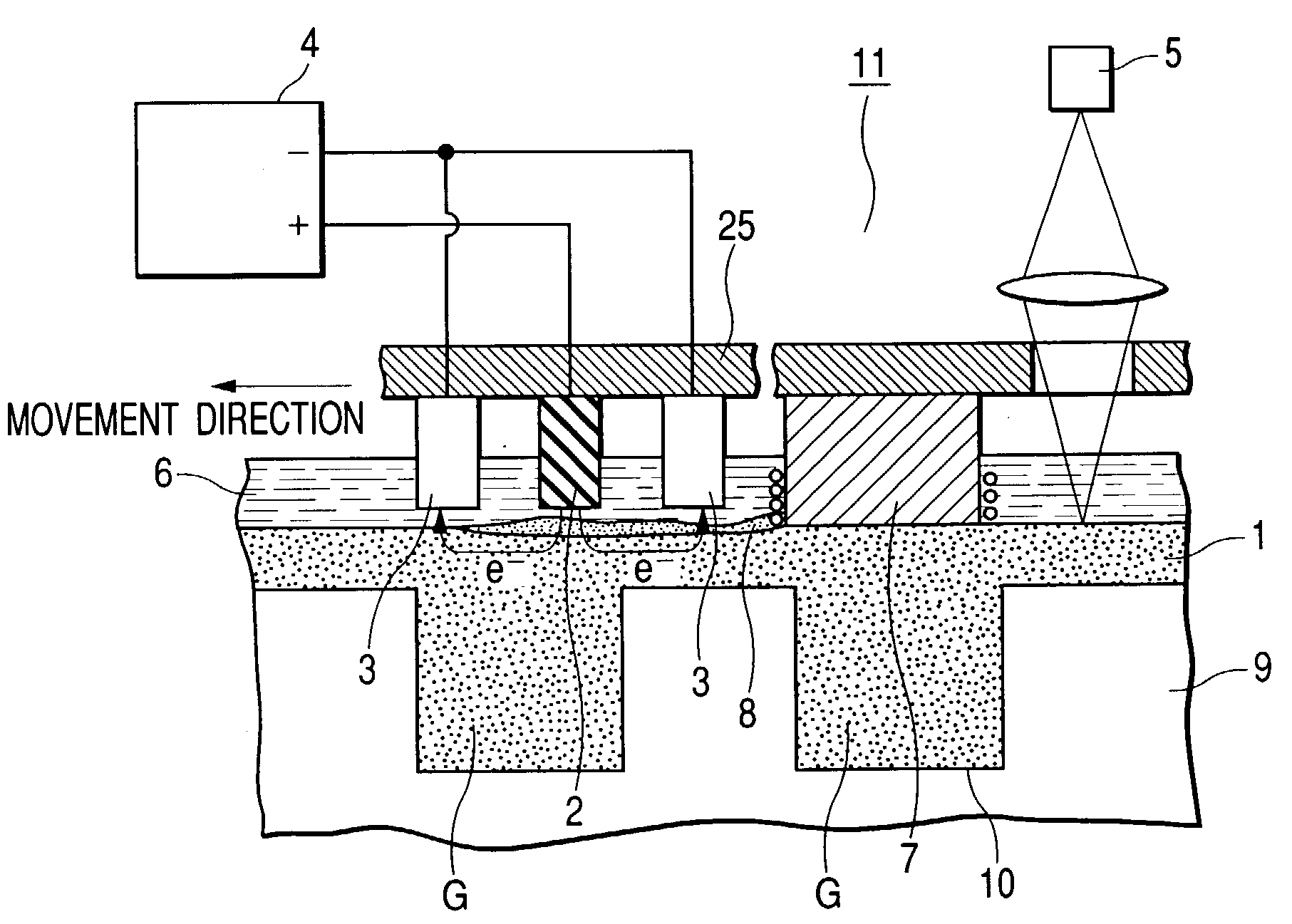
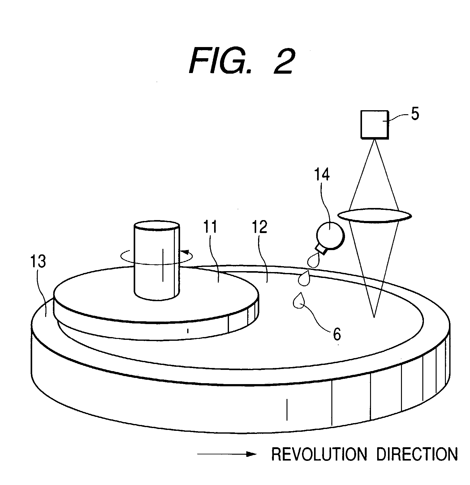
[0102] Next, referring to FIG. 6, an example in which the invention is applied to a processing apparatus for planarization provided with multiple platens will be described. A first platen 13-1 is composed of a grindstone 7, a linear electrolytic tool 18 and a linear image detector 19.

[0103] In the linear electrolytic tool 18, electrodes having the same structure as the unit of electrodes shown in FIGS. 3A and 3B concerning the first example, are linearly arrayed and also linearly arrayed the linear image detector 19, which are solid-state image sensing devices (CCDs).

[0104] A processing principle is similar to that in the first example, however, this example is different from the first example in that a polishing tool is larger than a wafer. The processing apparatus for planarization provided with the multiple platens in this example, has the similar structure to a so-called rotary CMP machine.

[0105] The processing apparatus for planarization in this embodiment is different from the...

first embodiment

[0106] Structure that the grindstone 7 is installed on the platen 13, the linear electrolytic tool 18 is linearly arranged on a radius and the linear image detector 19 is arranged on an another radius as shown in FIG. 7. The platen 13-1 and the second platen 13-2 have the similar structure. The linear electrolytic tool 18 is basically the same as the tool for-electro polishing in the first embodiment shown in FIGS. 1, 3A and 3B, though the linear electrolytic tool is different in the array of electrodes.

[0107] A third platen 13-3 is made of a normal polishing pad or a grindstone. A soft pad is mounted on the last fourth platen 13-4.

[0108] As shown in FIG. 6, a process--liquid--supplying nozzle 15 is provided to each platen and required solution is supplied at a required flow rate. The electro polishing of copper is enabled by such configuration as in the first embodiment.

[0109] Next, relationship between a processing process for planarizing copper damascene wiring and the apparatus ...

third example

[0118] FIG. 8 is a sectional view showing multilayer interconnection structure formed on a semiconductor substrate as an upper interconnection layer using processing technique for planarization according to the invention. That is, FIG. 8 shows a section of a multilayer interconnection logic device composed of six layers.

[0119] After a shallow trench is formed on the surface of a silicon wafer substrate 12 and an oxide film 21 is formed in the trench to construct a shallow trench isolation (STL) by processing technique for planarization, a gate pattern 22 is formed, and then,a transistor is formed. Afterward, a contact plug 23 made of tungsten (W) with an upper interconnection layer is formed by processing technique for planarizing W. A barrier film 24 is formed on an interface between the W plug 23 and a dielectric film 9 as in the copper interconnection structure. Layers on / over the W plug 23 are all a copper interconnection layer and these six interconnection layers 1-1 to 1-6 are...


PUM

PropertyMeasurementUnit
Electrical conductoraaaaaaaaaa
Electric potential / voltageaaaaaaaaaa
Heightaaaaaaaaaa

Abstract

The object of the invention is to provide a method of manufacturing a semiconductor device and a processing apparatus for planarization wherein to form copper wiring in multiple layers. The removal of a residue of polishing by local electro polishing, the enhancement of the performance of planarization by using a grindstone and the reduction by small frictional force in electro polishing of damage, are enabled. To achieve the object, the following measures are taken. A residue of polishing of copper is removed by combining the detection of a local area including the residue of polishing of copper and local processing for electro polishing. As small-load processing for planarization is enabled by using electro polishing, multilayer interconnection structure using low-k material as a dielectric interlayer is also enabled. Plural pairs of small unit electrodes in a pair of which minus electrodes surround a plus electrode are provided to a tool for electro polishing, each electrode is connected to a power supply, pulse voltage is applied to each electrode and copper is electrolytically polished.

Description

[0001] 1. Field of the Invention[0002] The present invention relates to a method for manufacturing a semiconductor device, particularly relates to a method for manufacturing a semiconductor device and a manufacturing apparatus respectively suitable for forming reliable wiring on a semiconductor substrate using technique for polishing and grinding in a damascene wiring forming process.[0003] 2. Description of the Related Art[0004] Recently, processing technique for planarization for shallow trench isolation (STI), forming a tungsten (W) plug for transmitting a signal from each transistor to an interconnection layer and forming the interconnection layer has been important for manufacturing a semiconductor integrated circuit.[0005] For the processing technique for planarization, polishing processing technique called chemical mechanical polishing (CMP) is representative.[0006] Particularly, lately copper is used for wiring material. For planarization, a damascene process is mainstream a...

Claims


Application Information

Patent Timeline
IPC IPC(8): B23H5/08B24B37/04C25F3/14C25F7/00H01L21/304H01L21/3205H01L21/321H01L21/768
CPCB23H5/08B24B37/04H01L21/7684C25F7/00H01L21/32125C25F3/14
Inventor KATAGIRI, SOUICHIYAMAGUCHI, UI
Owner RENESAS ELECTRONICS CORP
Why Eureka
Try Eureka