Clocked inverter, nand, nor and shift register

a technology of shift register and clock inverter, which is applied in the direction of generating/distributing signals, pulse techniques, instruments, etc., can solve the problems of increasing the occupation area of the driver circuit, reducing the frequency property, and increasing the total size of the device casing

Inactive Publication Date: 2004-04-01
SEMICON ENERGY LAB CO LTD
View PDF25 Cites 22 Cited by
  • Summary
  • Abstract
  • Description
  • Claims
  • Application Information

AI Technical Summary

Problems solved by technology

When level shifting is performed in an internal circuit, problems are caused, for example, in increase in occupation area of a driver circuit, reduction of frequency property due to delayed or blunted waveforms.
On the contrary, when a level shifter is arranged in an external circuit, problems are caused, for example, growth in total size of a casing for devices due to the increase in the number of components such as IC, in cost for manufacturing and in power consumption by the shift register.
As a result, such problems that the waveform of CK is delayed and blunted and that the voltage of a power source line arranged in the internal circuit is dropped are solved.
That is, there arises a problem that when a leak current is large, shift of pulse does not occur.
As a result, the overall load is increased and a high frequency operation is obstructed.
Two TFTs of the same conductive type connected in series are weak in current performance (power).
If the threshold value of the TFT 11 is lower than a desired value, there arises a case in which the TFT 11 is turned on an

Method used


Image

  • Clocked inverter, nand, nor and shift register
  • Clocked inverter, nand, nor and shift register
  • Clocked inverter, nand, nor and shift register

Examples


embodiment

[0176] Embodiment Mode 7

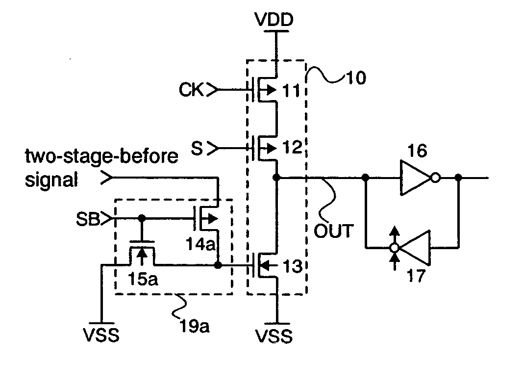
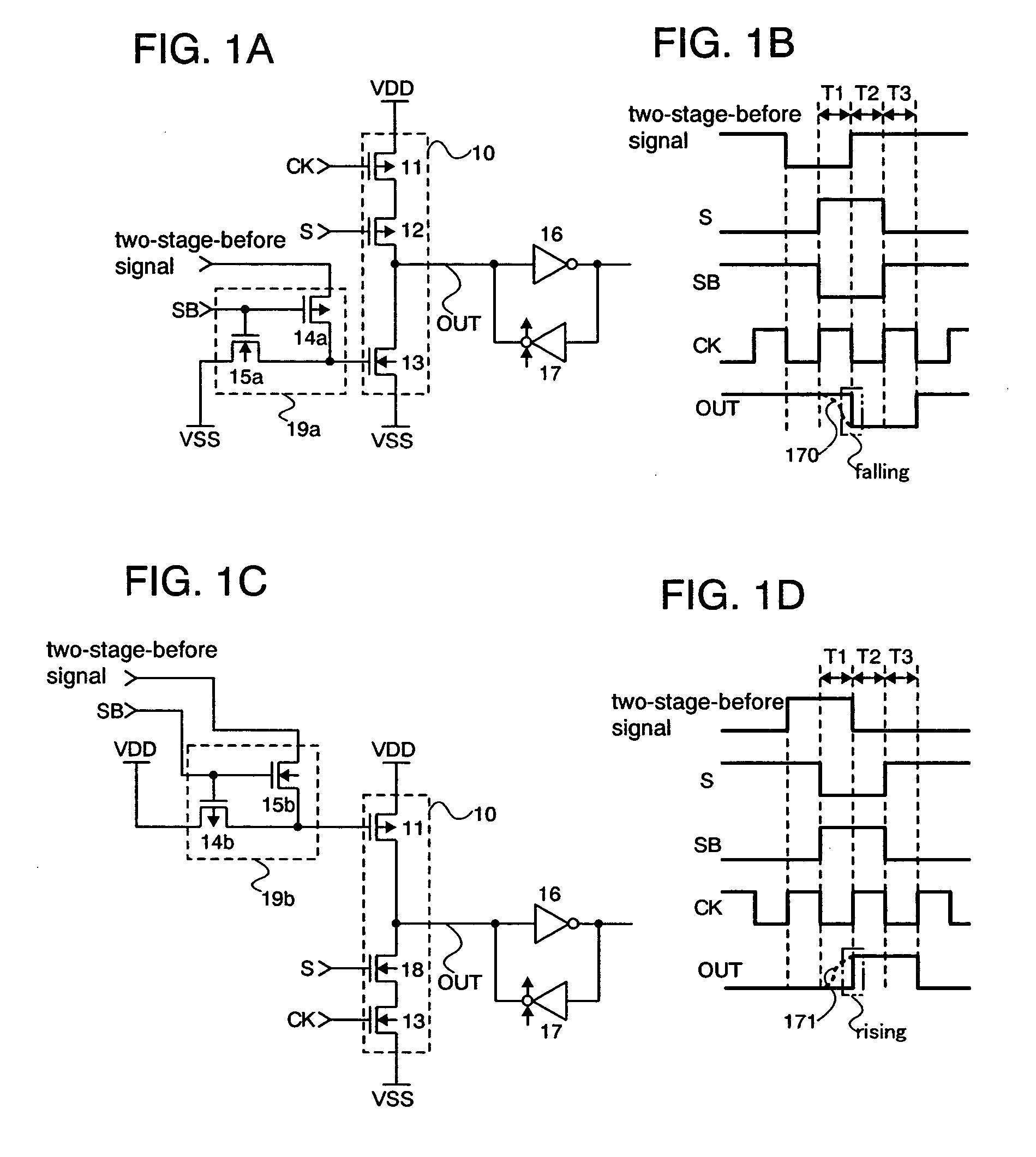
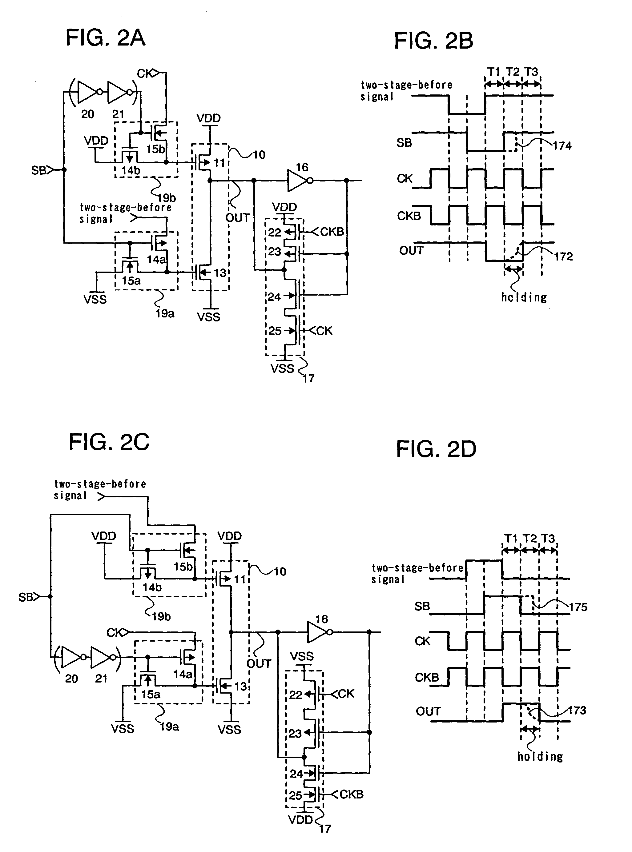
[0177] A seventh structure of the present invention will be described with reference to FIGS. 12A and 12B. FIG. 12A is a circuit diagram showing structural elements of a shift register arranged in the n-th stage. Each stage is formed by a clocked inverter 10 including TFTs 11 and 13 connected in series, a compensation circuit 19a including TFTs 14a and 15a, a compensation circuit 19b including TFTs 14b and 15b, a holding clocked inverter 17 including TFTs 24 and 181 connected in series, a compensation circuit including TFT 182 and an analog switch 184, and a compensation circuit including TFT 183 and an analog switch 185. The shift register is formed by cascade-connecting the respective stages, in which these circuits are arranged, with signals from CK and CKB being alternately inputted at the respective stages. This structure in FIG. 12A is different from the structure in FIG. 3A in that CKB is input to the source of TFT 14a instead of inputting two-stage-be...


PUM


Abstract

A threshold voltage of a transistor is fluctuated because of fluctuation in film thickness of a gate insulating film or in gate length and gate width caused by differences of used substrates or manufacturing steps. In order to solve the problem, according to the present invention, there is provided a clocked inverter including a first transistor and a second transistor connected in series, and a compensation circuit including a third transistor and a fourth transistor connected in series. In the clocked inverter, gates of the third transistor and the fourth transistor are connected to each other, drains of the third transistor and the fourth transistor are each connected to a gate of the first transistor, sources of the first transistor and the fourth transistor are each electrically connected to a first power source, a source of the second transistor is electrically connected to a second power source, and an amplitude of a signal inputted to a source of the third transistor is smaller than a potential difference between the first power source and the second power source.

Description

[0001] 1. Field of the Invention[0002] The present invention relates to a clocked inverter and also relates to a shift resister including a clocked inverter as a unit circuit. Further, the present invention relates to electric circuits such as a NAND and a NOR.[0003] 2. Description of the Related Arts[0004] In recent years, display devices such as a liquid crystal display device and a light emitting device have been developing greatly because of the growth in demand of mobile machines. A technique for integrating a pixel and a driver circuit (hereinafter, internal circuit) using a transistor formed of a polysilicon semiconductor on an insulator has been developing greatly, because the technique can contribute to miniaturization of devices and less electric power consumption. The internal circuit formed on an insulator is connected with a controller IC or the like (hereinafter, external circuit) thorough a FPC or the like to be controlled.[0005] Generally, the power source voltage of...

Claims


Application Information

Patent Timeline
IPC IPC(8): G11C19/00G09G3/20G11C19/28H03K19/003H03K19/096
CPCG11C19/00G11C19/28H03K19/0963H03K19/018521H03K19/00384G09G3/20
Inventor OSAME, MITSUAKIANZAI, AYA
Owner SEMICON ENERGY LAB CO LTD
Why Eureka
Try Eureka