Radiation detector, radiation detector element, and radiation imaging apparatus

a radiation detector and element technology, applied in the direction of optical radiation measurement, radiation controlled devices, instruments, etc., can solve the problems of low energy resolution, and even more deterioration in space resolution, so as to achieve the effect of raising the radiation space resolution

Inactive Publication Date: 2004-06-03
HITACHI LTD
View PDF2 Cites 26 Cited by
  • Summary
  • Abstract
  • Description
  • Claims
  • Application Information

AI Technical Summary

Benefits of technology

[0019] More preferably, the radiation detector comprises an element holding member (for example, detector module board) having: a plurality of holding units for detachably holding the radiation detector elements; and an electric connecting portion for electrically connecting anodes and cathodes of the radiation detector elements. An integrated circuit holding member (for example, ASIC module board) in which the element holding member and the integrated circuit (ASIC) have been installed is connected so that it can be separated. The semiconductor radiation detector element is set into a coaxial shape (shape in which a semiconductor device is arranged around (outer periphery) of a rod-shaped anode and a cathode is arranged around (outer periphery) of the semiconductor device) or a laminate structure. A shield of the radiation is arranged between the radiation detector elements. Thus, together with maintainability, the space resolution to the radiation can be raised.

Problems solved by technology

When the scintillator 31 is utilized, it detects the radiation via multi-level conversion from the radiation to the visible light and from the visible light to electrons, there is a problem such that energy resolution is low.
This kind of scattering radiation detection (refer to .gamma..sub.1' in FIG. 14) and causes a deterioration in space resolution.
Consequently, not only the space resolution deteriorates even more but a weight increases and maintenance efficiency of the radiation detector or the radiation imaging apparatus also deteriorates.
(1) An installing board of the detector and the ASIC are integratedly formed by bumping or the like and if one pixel is destroyed, the board has to be exchanged on a large unit basis. Since the detector element is very expensive, the exchange of the board on a large unit basis denotes that large costs are required.
(2) Also in view of the manufacturing of the camera, since the detector elements and the ASIC are installed onto one installing board, assembling steps of the camera are extremely complicated and, even if a defective element is found, it cannot be exchanged.
(3) Particularly in the radiation detector for imaging the high-energy .gamma.-ray, a length of collimator is long, a total length of radiation imaging apparatus is very long, and it is very heavy and large in size. This causes an enlargement in size of the apparatus in terms of intensity of structure members which support a camera unit and results in an increase in costs, a deterioration in maintenance efficiency, and an increase in anxiety of the patient.
In other words, it causes a deterioration in maintenance efficiency of the radiation detector and the radiation imaging apparatus.

Method used


Image

  • Radiation detector, radiation detector element, and radiation imaging apparatus
  • Radiation detector, radiation detector element, and radiation imaging apparatus
  • Radiation detector, radiation detector element, and radiation imaging apparatus

Examples


first embodiment

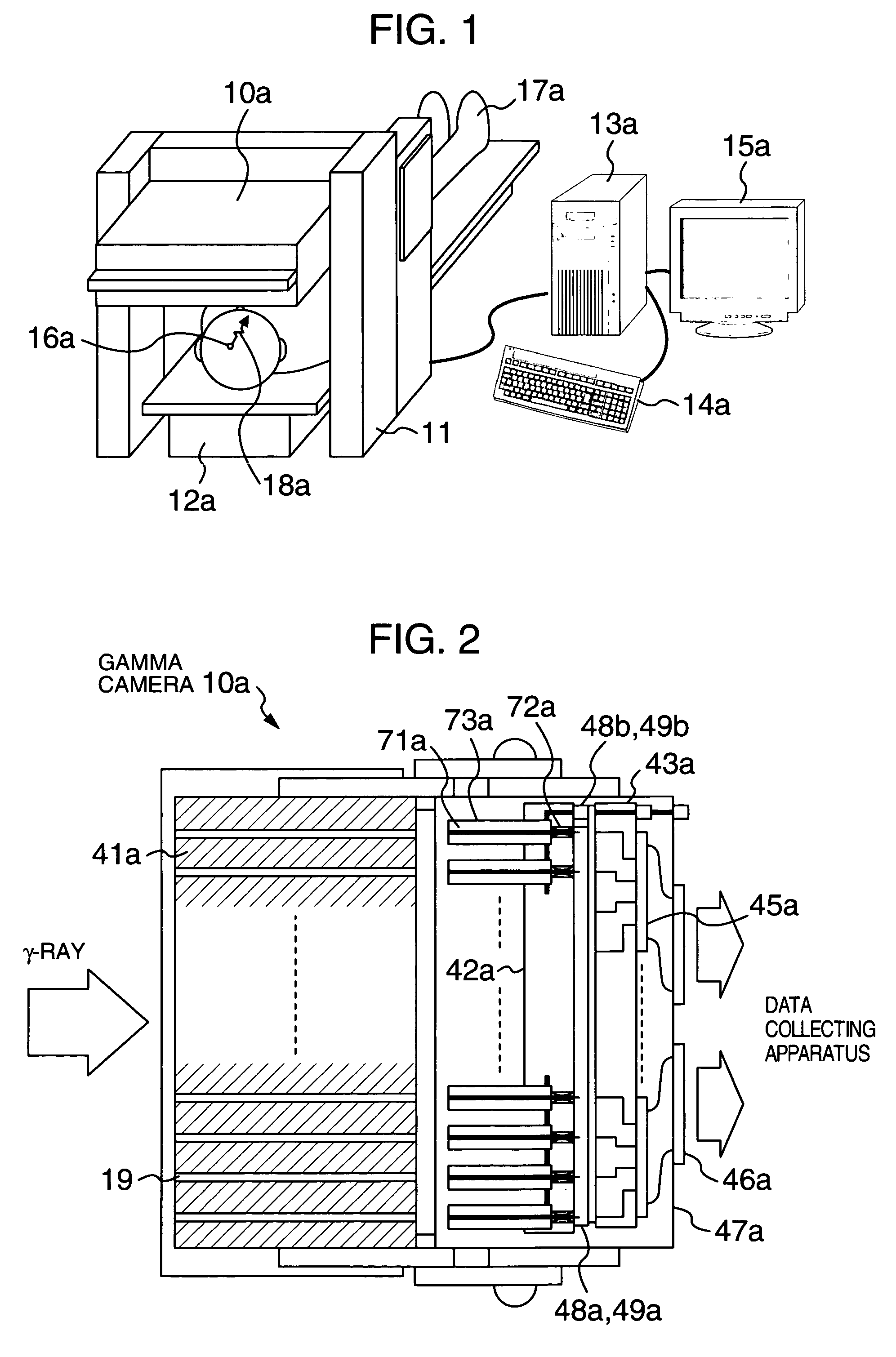
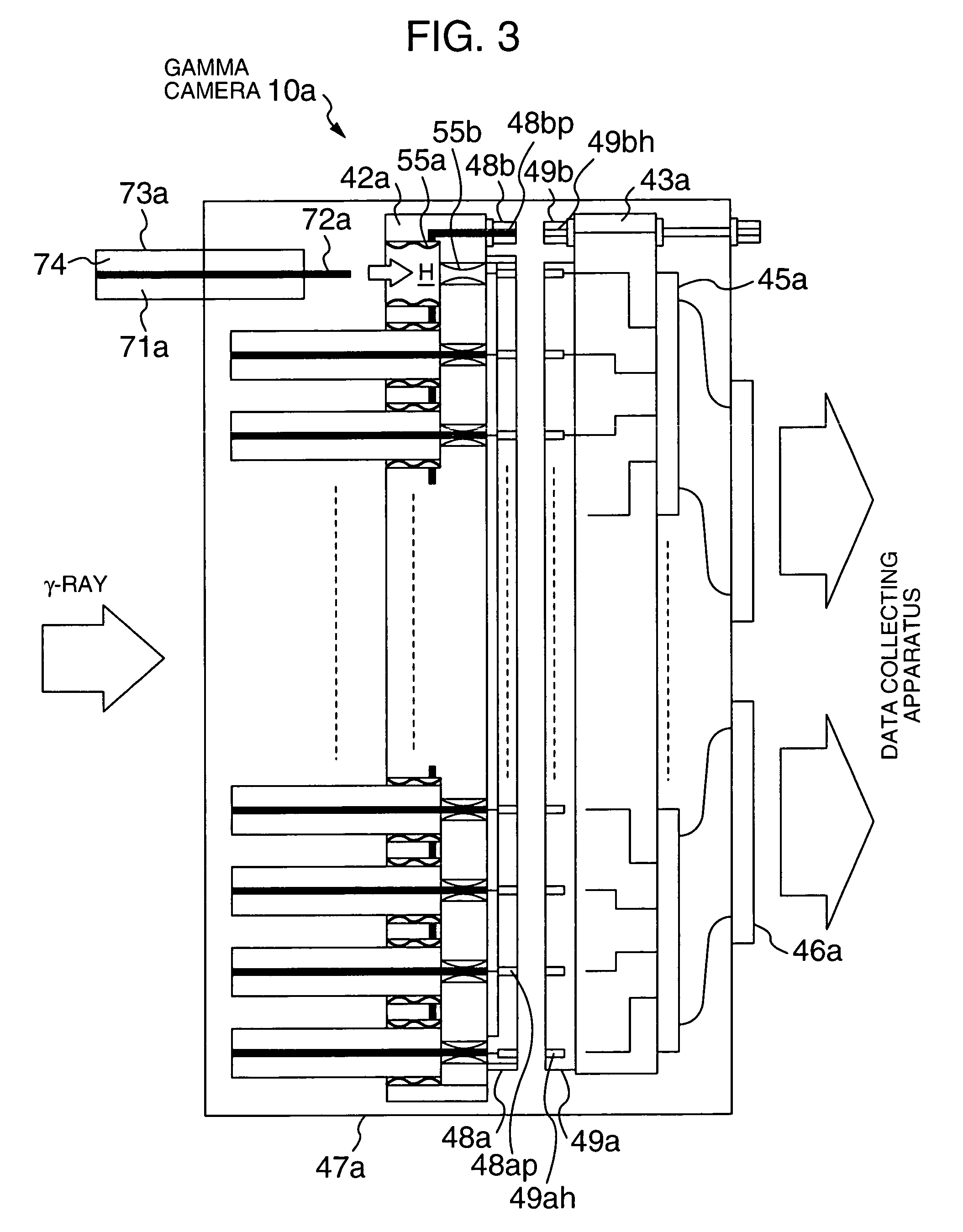
[0061] A gamma camera imaging apparatus of the first embodiment to improve maintenance performance or the like of a radiation detector by the attaching structure and the connecting structure will be described with reference to FIG. 1 and the like. FIG. 1 is a schematic side sectional view of a gamma camera.

[0062] Gamma Camera Imaging Apparatus (Radiation Imaging Apparatus)

[0063] A gamma camera imaging apparatus is a kind of nuclear medicine diagnosing apparatus. According to this apparatus, a radiomedicine dosed into a human body is accumulated or deposited in the body, a .gamma.-ray emitted from the radiomedicine is measured from a position out of the body, and a diagnosis is assisted on the basis of an accumulation degree or the like. For example, .sup.131I is dosed into the human body in a form of sodium iodide and an accumulation degree of sodium iodide accumulated in a thyroid gland is measured from a position out of the body, thereby examining a function of the thyroid gland.

[...

second embodiment

[0089] Subsequently, a gamma camera imaging apparatus of the second embodiment to improve the weight saving, downsizing and sensitivity or the like by saving (miniaturization) of collimators will be described with reference to FIG. 6 and the like.

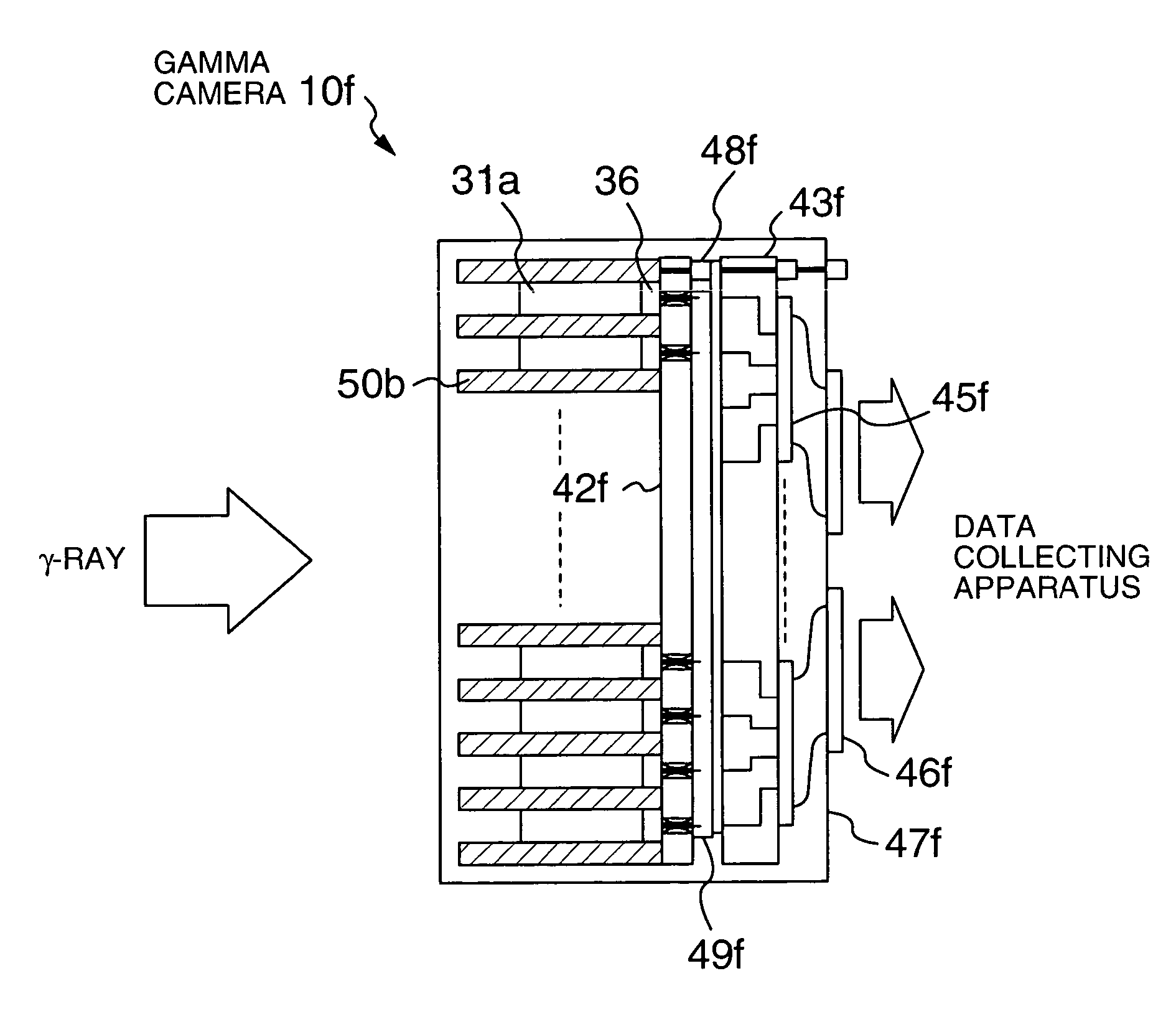
[0090] It is a large feature of a gamma camera 10d of the second embodiment shown in FIG. 6 that the collimator 41a (refer to FIG. 2 and the like) as shown in the first embodiment is omitted (made to be unnecessary). The gamma camera 10d has a lattice-shaped shield 50b constructing a plurality of holding portions H1 as through-holes. Each detector element 71a is fitted and held into each holding portion H1. That is, a whole periphery (excluding a front edge surface and a rear edge surface) of the detector element 71a is surrounded by the shield 50b. The shield 50b is made of a conductive radiation shielding material.

[0091] In association with the construction such that the detector element 71a is held by the shield 50b as mentioned above, a...

third embodiment

[0113] Subsequently, an embodiment regarding the structure of the detector elements which can be preferably used to the radiation detectors in the first and second embodiments will be described with reference to the drawings (properly refer to FIG. 18A and the like).

[0114] The detector element 71a in FIGS. 18A and 18B, the first embodiment (FIG. 3 and the like), and the second embodiment (FIG. 7 and the like) has a structure such that the pin-shaped anode (anode pin) 72a is arranged on a center axis, the semiconductor device 74 surrounds a periphery of the anode 72a, and a whole side surface of the semiconductor device 74 is the cathode 73a. An ordinary detector element 171e as shown in FIGS. 19A and 19B has a structure such that electrodes 172e and 173e are provided on both surfaces of a plate-shaped semiconductor device 76 called a planer type. To completely collect the charges generated due to the extinction of the .gamma.-ray in the semiconductor device 76 of the detector elemen...


PUM


Abstract

In a gamma camera, a plurality of radiation detector elements having a rod-shaped first electrode, a semiconductor device surrounds the first electrode to contact with it for entering a radiation, and a second electrode provided for the side surface of the semiconductor device are detachably attached to a holding member. The holding member has a first electrode contact portion contacted with the first electrode and a second electrode contact portion contacted with the second electrode. A collimator in which a plurality of radiation paths provided corresponding to the plurality of radiation detector elements are formed is arranged on the radiation entering side of the plurality of radiation detector elements. A gamma-ray detection signal outputted from the first electrode contact portion is sent to a signal processing integrated circuit. A high voltage is applied to the second electrode via the second electrode contact portion.

Description

[0001] 1. Field of the Invention[0002] The invention relates to detection and an imaging operation of a radiation such as X-ray, .gamma.-ray, or the like and, more particularly, to a radiation detector, a radiation detector element, and a radiation imaging apparatus for detecting a .gamma.-ray of high energy.[0003] 2. Description of the Related Art[0004] When taking a medical X-ray as an example, as well as a radiation imaging apparatus of a film type, radiation imaging apparatuses such as imaging plate and flat panel detector (FPD) having both excellent resolving power and resolution have been developed. As a detector element, there has been used: a scintillation detector formed by combining a scintillator which reacts on a radiation and emits light and a photomultiplier or a photodiode which converts the light into charges; or a solid state device such as a semiconductor radiation detector which reacts on the radiation and directly collects generated charges or the like. For examp...

Claims


Application Information

Patent Timeline
Patent Type & Authority Applications(United States)
IPC IPC(8): G01J1/00G01T1/24G01T1/161G01T1/29H01L25/00
CPCG01T1/2928A61B6/42G01T1/20G01T1/241G01T1/20187
Inventor TSUCHIYA, KATSUTOSHIKITAGUCHI, HIROSHIYOKOI, KAZUMAUMEGAKI, KIKUOAMEMIYA, KENSUKEUENO, YUUICHIROUYANAGITA, NORIHITOKOJIMA, SHINICHI
Owner HITACHI LTD
Why Eureka
Try Eureka