Triode structure of field emission display and fabrication method thereof
a technology of field emission display and triode structure, which is applied in the manufacture of electric discharge tubes/lamps, tubes with screens, and discharge tubes luminescnet screens
- Summary
- Abstract
- Description
- Claims
- Application Information
AI Technical Summary
Problems solved by technology
Method used
Image

Examples
first embodiment
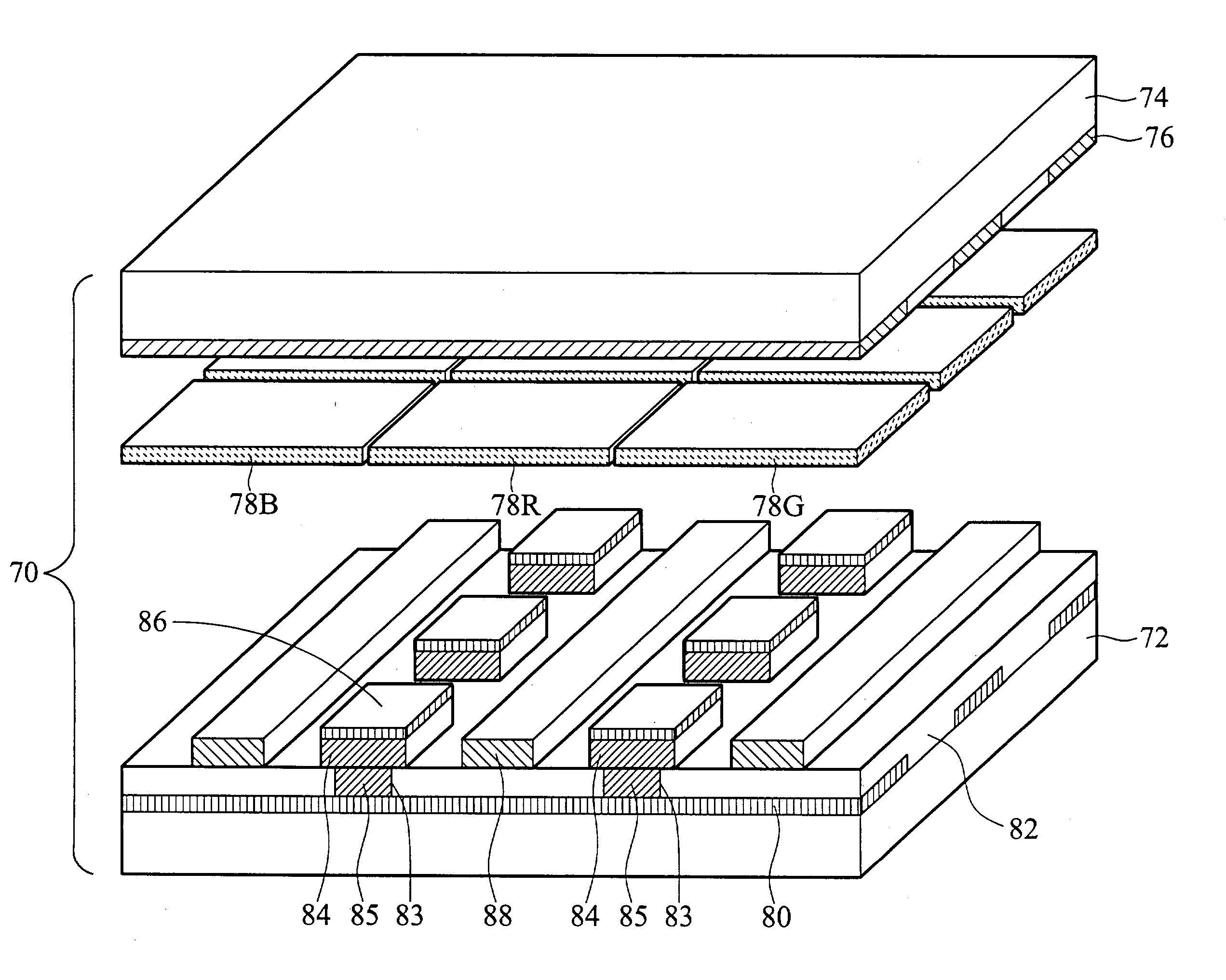
[0029] FIG. 4A is a solid diagram showing a triode structure of a FED device according to the present invention. FIG. 4B is a sectional diagram of the triode structure shown in FIG. 4A.
[0030] A FED device 70 is constituted by a lower substrate 72 and an upper substrate 74 arranged in parallel to each other. Preferably, glass panel material is used to form the two substrates 72 and 74. Alternatively, a transparent insulating material is used to form the two substrates 72 and 74. In addition, a spacer is provided in the vacuum between the two substrates 72 and 74 for maintaining a predetermined vertical distance and resisting atmospheric pressure.
[0031] The upper substrate 74, serving as an anode substrate, comprises a plurality of transverse-extending anode layers 76 and a plurality of fluorescent layers 78 arranged in a matrix formed on the inner surface thereof. Preferably, the anode layer 76 is ITO, and the fluorescent layer 78 consists of a red fluorescent layer 78R, a green fluo...
second embodiment
[0039] FIG. 6A is a solid diagram showing a triode structure of a FED device according to the second embodiment of the present invention. FIG. 6B is a sectional diagram of the triode structure shown in FIG. 6A.
[0040] According to the electrode structure on the lower substrate 72 described in the first embodiment, the second embodiment modifies the cathode layer 84 and the emitting layer 86 to make the periphery of the gate layer 88 within one pixel area overall surrounded by the emitting layer 86.
[0041] The lower substrate 72 serves as a cathode substrate. A plurality of lengthwise-extending conductive layers 80 is patterned on the inner surface of the lower substrate 72. A first dielectric layer 82I is deposited on the conductive layers 80 and the lower substrate 72, and has a plurality of openings 83 to expose portions of the conductive layers 80 for electrically connecting cathode layers. A plurality of contact layers 85 is formed in the openings 83, respectively, to be electrica...
third embodiment
[0048] FIG. 8 is a solid diagram showing a triode structure of a FED device according to the third embodiment of the present invention.
[0049] In accordance with the electrode structure on the lower substrate 72 described in the second embodiment, the third embodiment further modifies the emitting pattern 86 as a plurality of emitting elements 86A, 86B, 86C and 86D arranged in a matrix without connecting to each other. Preferably, the emitting element 86B or 86D is formed on the electron-emitting area of the first cathode layer 84I, and the emitting element 86A or 86C is formed on the electron-emitting area of the second cathode layer 84II. Thus, within one pixel area, the four lateral regions (ahead, right, behind and left regions) of the gate layer 88 are surrounded by the four emitting elements 86A, 86B, 86C, and 86D, respectively. The design choices consisting of area, profile and interval of the emitting elements 86A, 86B, 86C and 86D are not limited in the present invention.
PUM
 Abstract
Description
Claims
Application Information
 - R&D
- Intellectual Property
- Life Sciences
- Materials
- Tech Scout
- Unparalleled Data Quality
- Higher Quality Content
- 60% Fewer Hallucinations
Browse by: Latest US Patents, China's latest patents, Technical Efficacy Thesaurus, Application Domain, Technology Topic, Popular Technical Reports.
© 2025 PatSnap. All rights reserved.Legal|Privacy policy|Modern Slavery Act Transparency Statement|Sitemap|About US| Contact US: help@patsnap.com