Apparatus and techniques for scanning electron beam based chip repair

a scanning electron beam and chip technology, applied in the field of semiconductor chip repair and editing, can solve the problems of gallium contamination, physical sputtering of the sample surface, and damage to the sample surfa

Inactive Publication Date: 2004-06-17
GLOBALFOUNDRIES US INC
View PDF2 Cites 58 Cited by
  • Summary
  • Abstract
  • Description
  • Claims
  • Application Information

AI Technical Summary

Problems solved by technology

However, exposure to these highly energetic ion beams often causes IC damage, gallium contamination, and physical sputtering of the sample surface whereby the actual amount of material removed by such sputtering depends on the total ion dose and energy at each pixel location.
Further, a significant amount of the sputtered material is undesirably re-deposited onto adjacent areas.
This re-deposition slows the rate at which material can be removed, limits the maximum achievable aspect ratio of holes and openings created by FIB, and can adversely affect the electrical properties of the IC under edit.
However, it has been found that gas-assisted etching cannot completely address these issues, due to the continued dependence of FIB on gallium ion based beams for inducing these reactions.
In recent years, the introduction of copper for interconnect metallization has presented additional problems in the processes of chip repair and editing using existing FIB tools and techniques, including those having gas-assisted etching (GAE) options.
In the case of copper interconnect metalization editing, ion beam compatible gas chemistries have not been determined for complete volatilization of the etch products, which leads to re-deposition of conductive copper by-products onto adjacent areas and degradation of the IC's electrical performance.
The IC interconnect is then cut by milling the metal feature (e.g. copper) with little chemical assistance, as there is currently no completely effective ion beam compatible chemistries for volatilization of the metal etch by-products, particularly in the case of copper.
Another common repair scenario involves clearing large surface area

Method used


Image

  • Apparatus and techniques for scanning electron beam based chip repair
  • Apparatus and techniques for scanning electron beam based chip repair
  • Apparatus and techniques for scanning electron beam based chip repair

Examples


Embodiment Construction

(s)

[0037] In describing the preferred embodiment of the present invention, reference will be made herein to FIGS. 1-14 of the drawings in which like numerals refer to like features of the invention. Features of the invention are not necessarily shown to scale in the drawings.

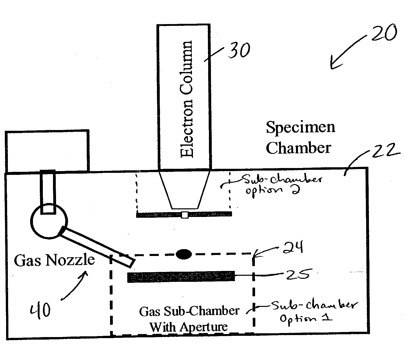
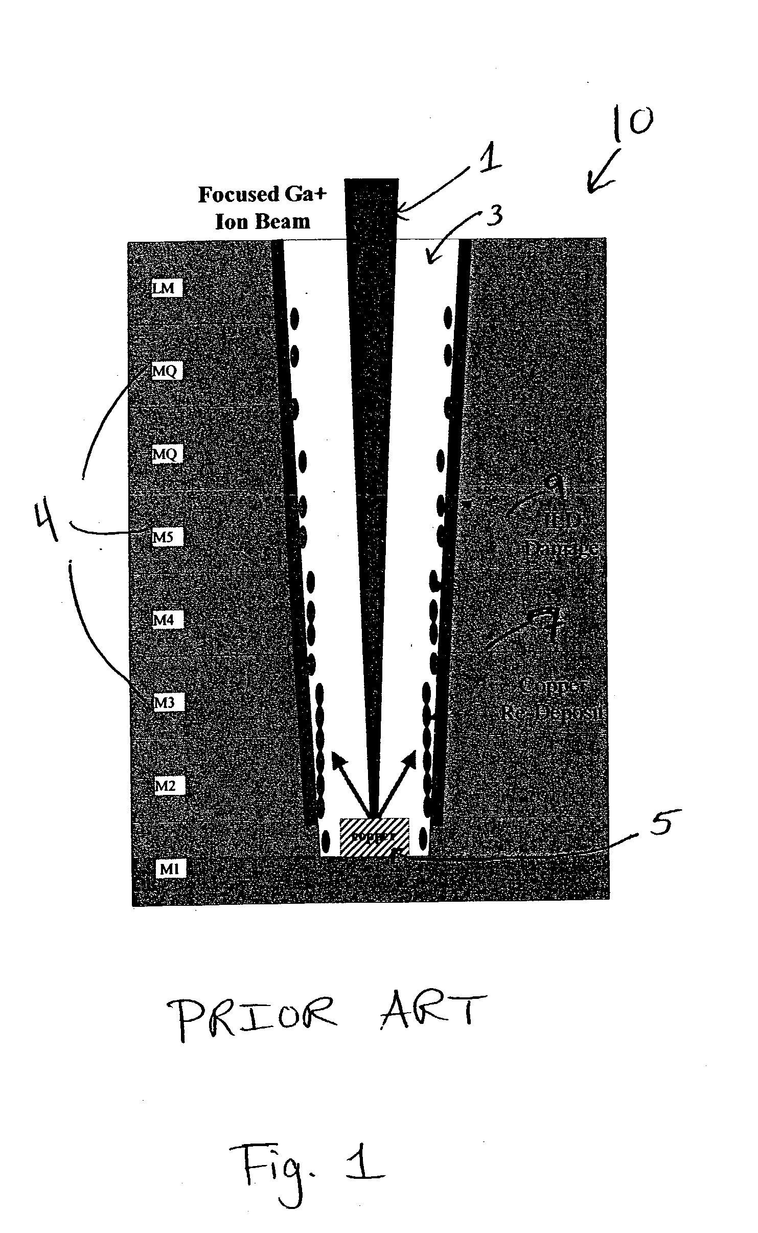
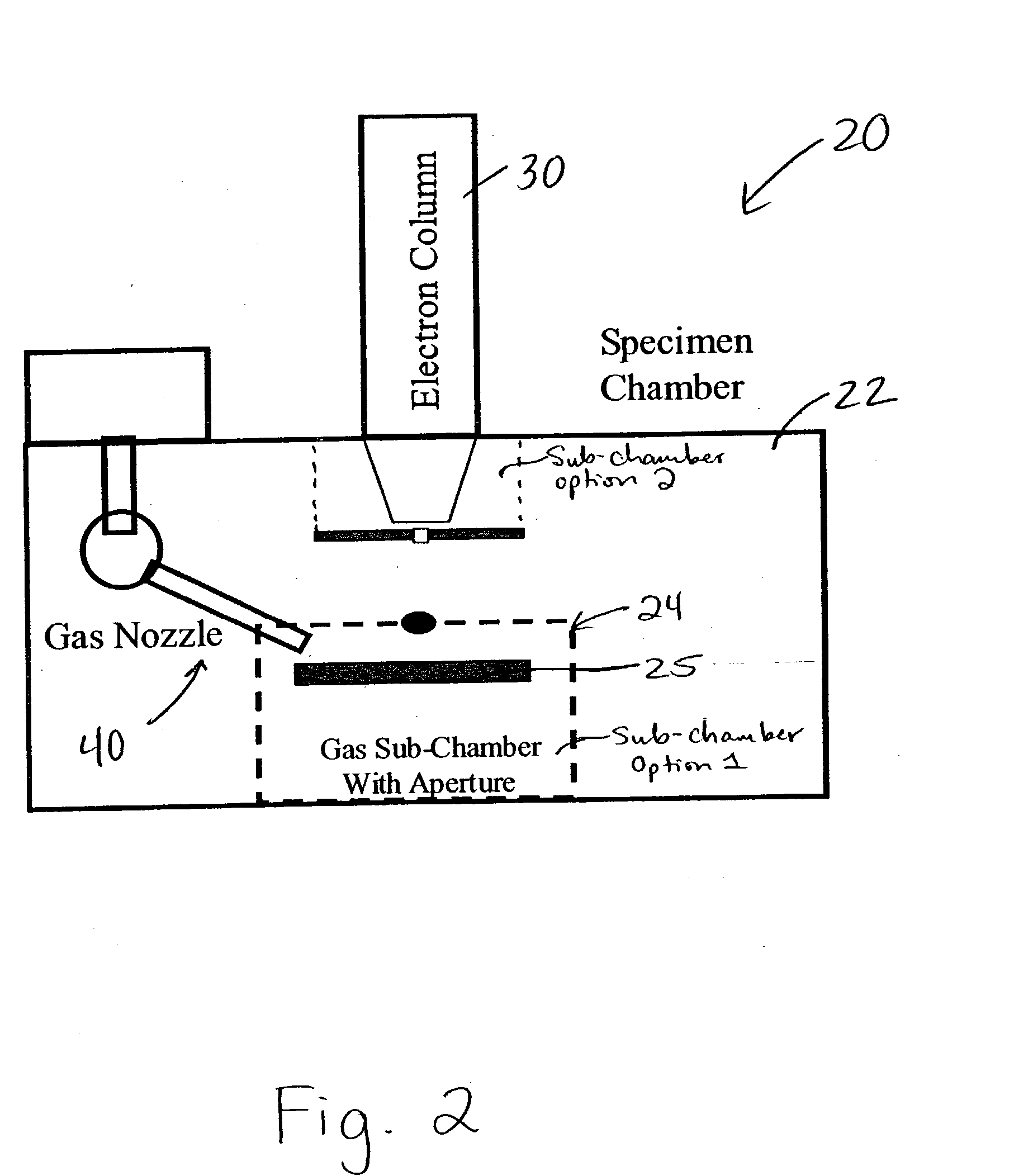
[0038] The present invention is directed to an apparatus and methods for repairing integrated circuits (ICs), wherein repairing encompasses the editing and prototyping of such ICs, using electron-beam-induced chemical processes that may be assisted with low-energy ions, or optically with focused light. The invention overcomes the above problems associated with conventional apparatus and techniques for repairing and editing ICs, such as liquid metal based focused ion beam (FIB) induced processes. These problems include, but are not limited to, IC electronic device damage, wafer surface contamination, re-deposition of conductive metal interconnect byproducts that can electrically short IC features, and damage of t...


PUM


Abstract

A method and apparatus for editing an integrated circuit by bombarding a feature in need of editing with either a low-energy or high-energy electron beam in the presence of a gas whereby low energy electrons activate reactants adsorbed on the surface of the feature in need of editing to form active species on the feature surface. The reaction products from the process can be easily removed whereby IC damage, leakage between metal features, wafer contamination and physical sputtering of undesired material can be significantly minimized while still possessing nanometer-scale spatial resolution. The low energy electrons for activating the reactants adsorbed on the surface of the feature to be edited may be emitted from the electron beam itself or they may be secondary low energy electrons emitted from the surface of the feature being edited.

Description

[0001] 1. Field of the Invention[0002] The present invention relates generally to semiconductor chip repair and editing, and in particular, to apparatus and processes for editing and repairing integrated circuits having copper and / or organic-based features.[0003] 2. Description of Related Art[0004] Present processes for integrated circuit (IC) repair and editing primarily rely on the use of focused ion beams for spatially localized removal and deposition of materials. These beams are generated by a Focused Ion Beam (FIB) tool which utilizes a liquid metal ion source, typically gallium (Ga+), from which highly energetic beams (E>30 keV) are formed and then focused onto the sample surface by electrostatic lenses. However, exposure to these highly energetic ion beams often causes IC damage, gallium contamination, and physical sputtering of the sample surface whereby the actual amount of material removed by such sputtering depends on the total ion dose and energy at each pixel locati...

Claims


Application Information

Patent Timeline
IPC IPC(8): H01J37/305
CPCH01J2237/31744H01J37/3056
Inventor MARCHMAN, HERSCHEL M.SHORE, AARON D.
Owner GLOBALFOUNDRIES US INC
Why Eureka
Try Eureka