Method for manufacturing CMOS image sensor using spacer etching barrier film

a technology of cmos image sensor and spacer, which is applied in the field of method for fabricating cmos image sensor, can solve the problems of limiting the effect of these efforts, defects in crystal lattice structure, and dark current, and achieve the effect of reducing dark current and improving the optical properties of short wavelength ligh

Inactive Publication Date: 2004-07-08
CARL ZEISS SMT GMBH +1
View PDF3 Cites 45 Cited by
  • Summary
  • Abstract
  • Description
  • Claims
  • Application Information

AI Technical Summary

Benefits of technology

[0016] In order to solve the above described problems, a manufacturing method for CMOS image sensor is disclosed that reduces dark current by protecting the surface of the photodiode from the blanket dry etching using spacer etching barrier film, and therefore improves the optical properties for short wavelength light using a spacer forming insulation layer residual on the surface of the photodiode.

Problems solved by technology

However, since the logic circuit part is indispensable, there is a limit to what these efforts can achieve.
At this time, the surface of the photodiode can get damaged during the blanket dry etching process, causing defects in the crystal lattice structure.
This dark current is reported to be caused by various defects (line defect, point defect, etc.) or dangling bonds, existing near the edge of the active area.
The dark current can be a serious problem in low illumination environment.
According to the above described prior art, there is the problem that during the blanket etching for spacer formation, the surface of the photodiode becomes damaged, and dangling bonds existing on the damaged surface could cause dark current.
When the light passes from a low reflection coefficient material like the oxide to a high reflection coefficient material like the epitaxial layer, there is the problem that short wavelength lights like blue is reflected away, so photosensitivity becomes low.

Method used


Image

  • Method for manufacturing CMOS image sensor using spacer etching barrier film
  • Method for manufacturing CMOS image sensor using spacer etching barrier film
  • Method for manufacturing CMOS image sensor using spacer etching barrier film

Examples


Embodiment Construction

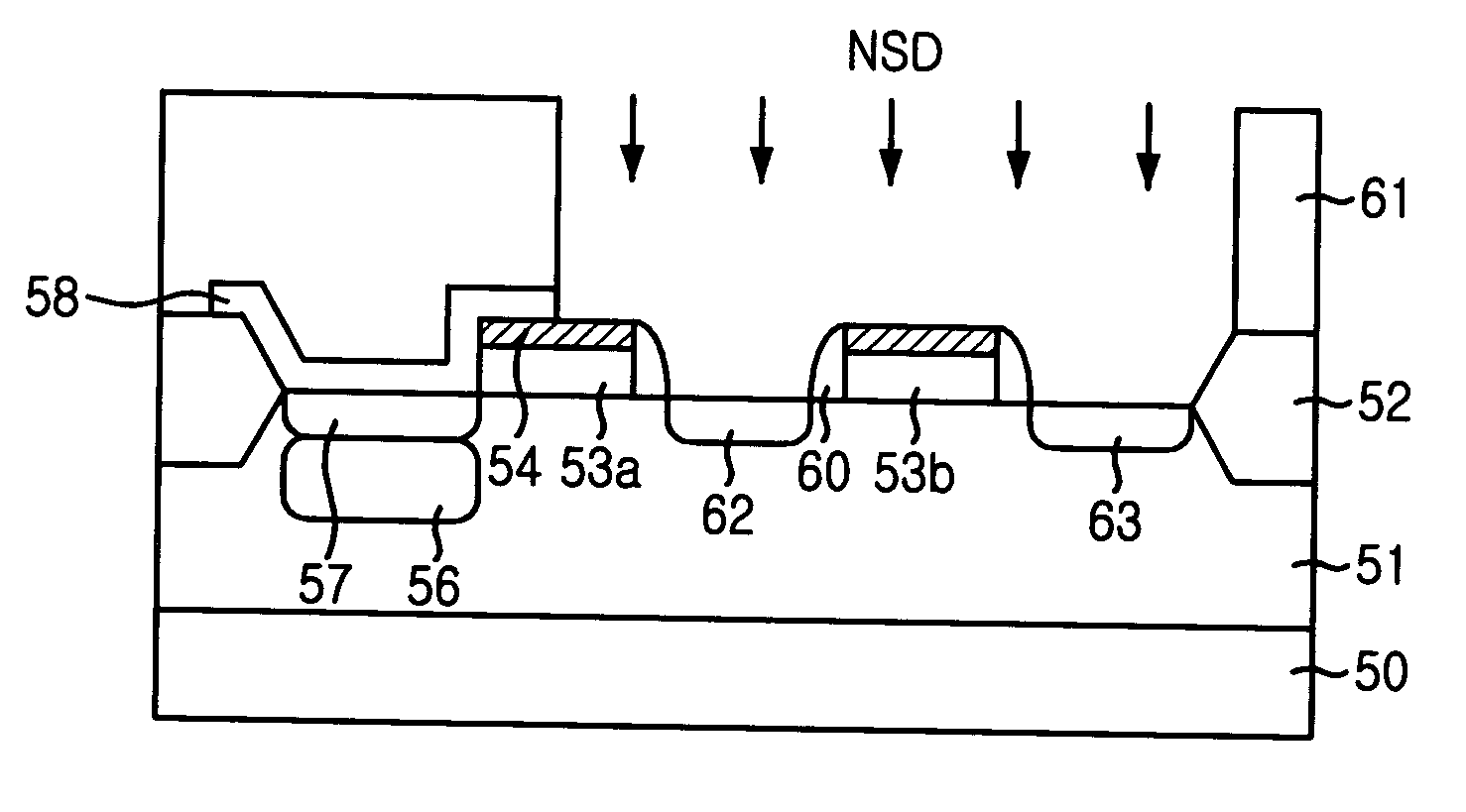
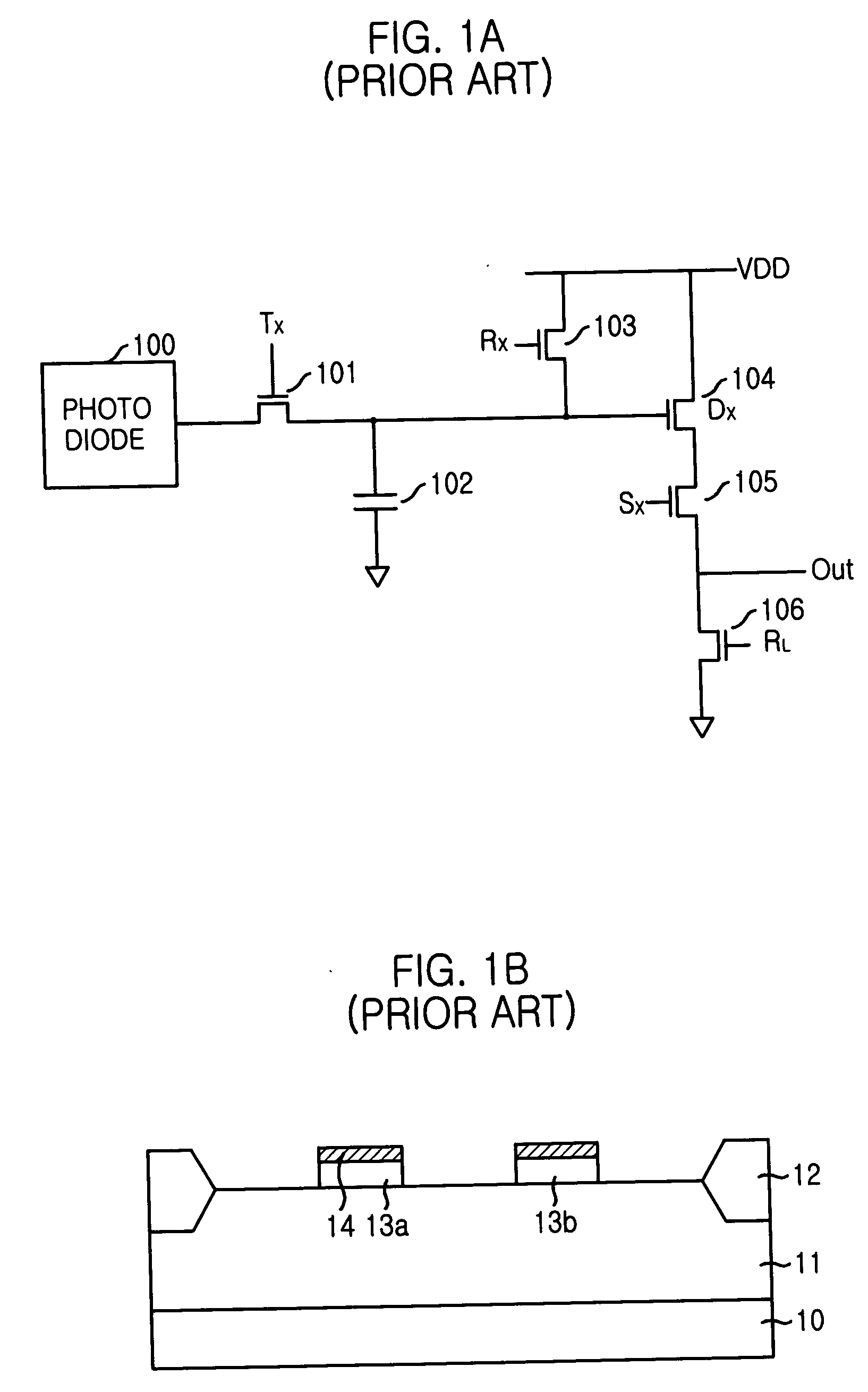
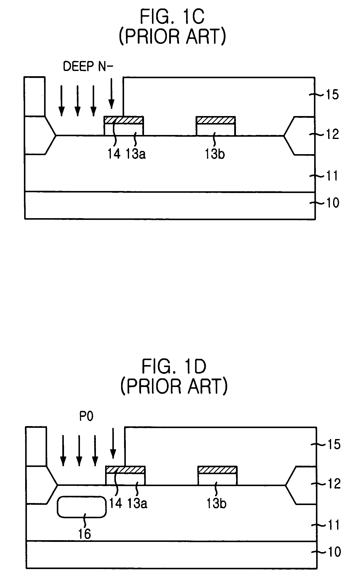
[0025] FIG. 2A through 2F are cross-sectional views of disclosed manufacturing process of a CMOS image sensor with emphasis on the transfer transistor and reset transistor.

[0026] First, a lightly doped p-type epitaxial layer 31 is formed on the heavily doped p-type substrate 30 as shown on FIG. 2A. This combination is used because the lightly doped epitaxial layer 31 improves the performance characteristics by increasing the depth of the depletion layer, and the heavily doped substrate 30 prevents crosstalk between unit pixels.

[0027] Next, a component isolator 32 is formed on some area of the epitaxial layer 31. In an embodiment, a field oxide using thermal oxide can be used as component isolator, however, it is possible to use trench structure as a component isolator.

[0028] Next, the gates of the transfer transistor 33a and the reset transistor 33b are formed on the active area by depositing gate oxide (not shown), gate polysilicon 33, and tungsten silicide 34 and by patterning the...


PUM


Abstract

A method for fabricating a CMOS image sensor including a low voltage buried photodiode and a transfer transistor, includes the steps of: forming a field oxide for defining active area and field area on certain area of an epitaxial layer formed on a substrate, and forming a gate of transfer transistor on the epitaxial layer of the active area; forming the low voltage buried photodiode doping region in alignment with one side of the gate of transfer transistor and field oxide; forming a spacer insulation layer by stacking layers of oxide and nitride over the whole structure; forming a spacer block mask to open areas excluding doping region for the low voltage buried photodiode; and removing the spacer block mask, and forming a floating diffusion region on other side of the transfer transistor. Alternatively, the sacrificial nitride may be allowed to remain on the surface of the photodiode to improve optical properties for short wavelength lights.

Description

[0001] 1. Technical Field[0002] A method for fabricating a CMOS image sensor is disclosed and, more particularly a method for fabricating a CMOS image sensor is disclosed that reduces the amount of dark current by protecting the surface of a photodiode with spacer etching barrier film during the etching process for formulation of spacers.[0003] 2. Description of the Related Art[0004] In general, an image sensor is a semiconductor device that converts an optical image into electrical signals. In a charge coupled device (CCD), a plurality of Metal-Oxide-Silicon (MOS) capacitors is placed in close proximity, and charge carriers are stored in or transferred between capacitors. CMOS image sensors are devices using as many MOS transistors as the number of pixels to detect output sequentially, and is based on CMOS technology that uses peripheral circuits such as control circuits and signal processing circuits.[0005] As is well known, an image sensor for color images has a color filter arra...

Claims


Application Information

Patent Timeline
Patent Type & Authority Applications(United States)
IPC IPC(8): H01L21/00H01L21/8238H01L27/14H01L27/146H01L31/00H04N5/335H04N5/361H04N5/369H04N5/374
CPCH01L27/14689H01L27/14609
Inventor LEE, JU-IL
Owner CARL ZEISS SMT GMBH
Why Eureka
Try Eureka