High power semiconductor laser with a large optical superlattice waveguide

a superlattice waveguide, high-power semiconductor technology, applied in semiconductor lasers, laser details, electrical equipment, etc., can solve the problem of difficult to achieve good composition control, achieve low vertical farfield, reduce optical losses, and reduce optical loss

Active Publication Date: 2004-10-21
LUMENTUM TECH UK LTD +1
View PDF4 Cites 35 Cited by
  • Summary
  • Abstract
  • Description
  • Claims
  • Application Information

AI Technical Summary

Benefits of technology

[0025] The novel high power laser structure according to the invention has a continuous active region comprising a gain region and a waveguide and an optical waveguide in the cladding whose vertical part consists or comprises an optical superlattice, whereby the superlattice itself consists of or includes an arrangement of layers with alternating indices of refraction. This enables a low vertical farfield and reduced optical losses, as needed for high power operation, e.g. as pump sources for Raman amplifiers. The large optical superlattice (LOSL) is designed to produce the desired low vertical farfield by weak vertical guiding of the optical mode which results in a widened nearfield mode. This is due to the low average index of refraction obtained from the individual layers of the large optical superlattice (LOSL).
[0026] The provision of a LOSL in the laser structure overcomes the problems associated with the growth of material having a low index of refraction, i.e. close to the value for the cladding layers. This is especially the case for quaternary alloys, e.g. in the material system InP / InGaAsP for quaternary alloys with photoluminescence wavelength significantly smaller than 1100 nm. In this wavelength region, it is well known that good control of the composition is hard to achieve. With the present invention, the individual layers of the LOSL are made of material whose composition is easy to control, and the layers have dimensions in the material-wavelength of the light or smaller, i.e. the wavelength in vacuum divided by the index of refraction of the material. Therefore, an averaging of the optical properties occurs while the electronic properties remain those of the individual layers. Varying the thickness of the individual layers allows an easy adjustment of the LOSL's average index of refraction. It also allows a profile shaping of the guided zero and higher order modes by intentional thickness variations.
[0027] Using this technique allows the relative simple fabrication of large optical waveguides with constant, or linearly graded (G-LOSL), or arbitrarily shaped (S-LOSL) index profiles. The LOSL is especially advantageous for structures which support asymmetric guiding of the mode, i.e. where the mode is guided mainly in the n-doped part of the laser structure to reduce free-carrier absorption. This can be achieved by an asymmetric large optical superlattice (A LOSL).

Problems solved by technology

In this wavelength region, it is well known that good control of the composition is hard to achieve.

Method used


Image

  • High power semiconductor laser with a large optical superlattice waveguide
  • High power semiconductor laser with a large optical superlattice waveguide
  • High power semiconductor laser with a large optical superlattice waveguide

Examples


Embodiment Construction

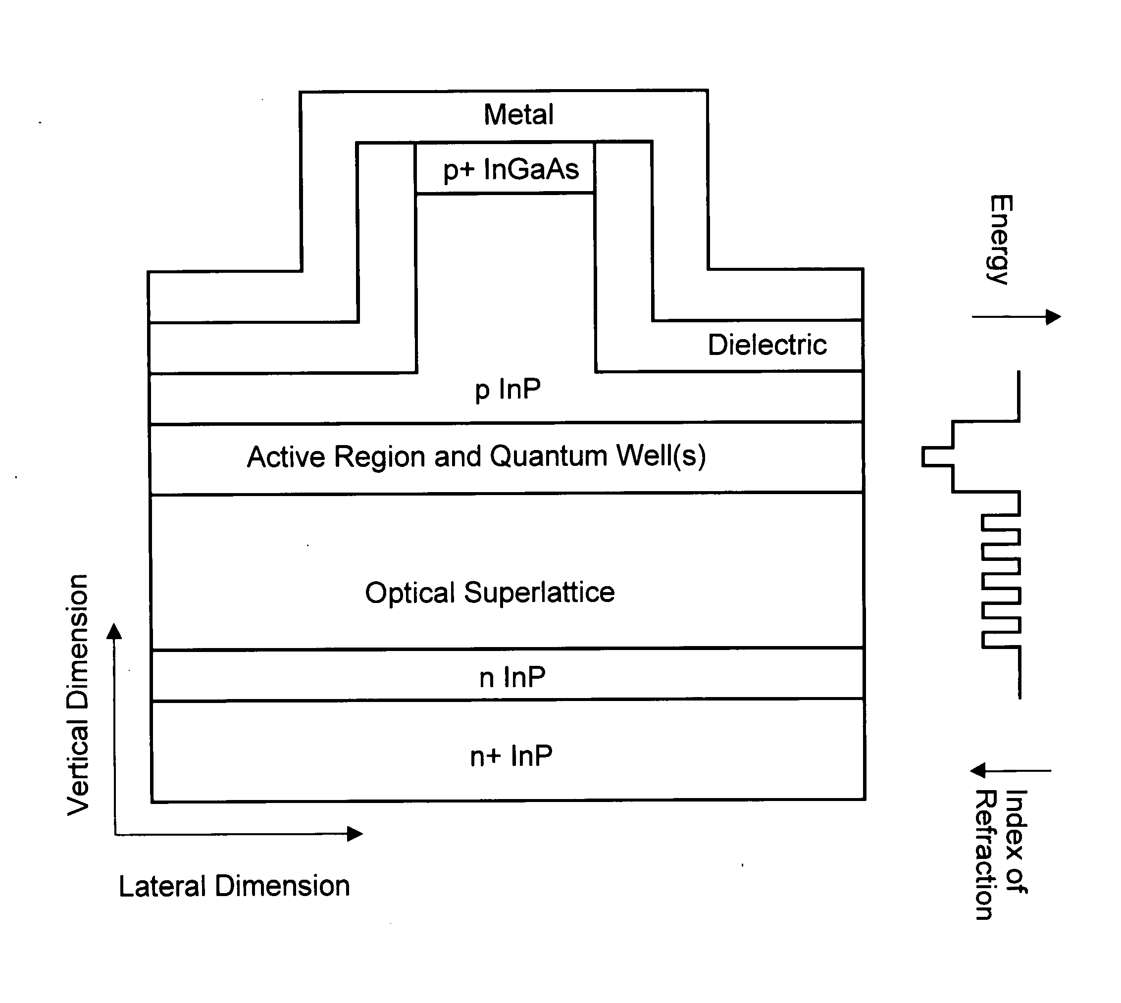
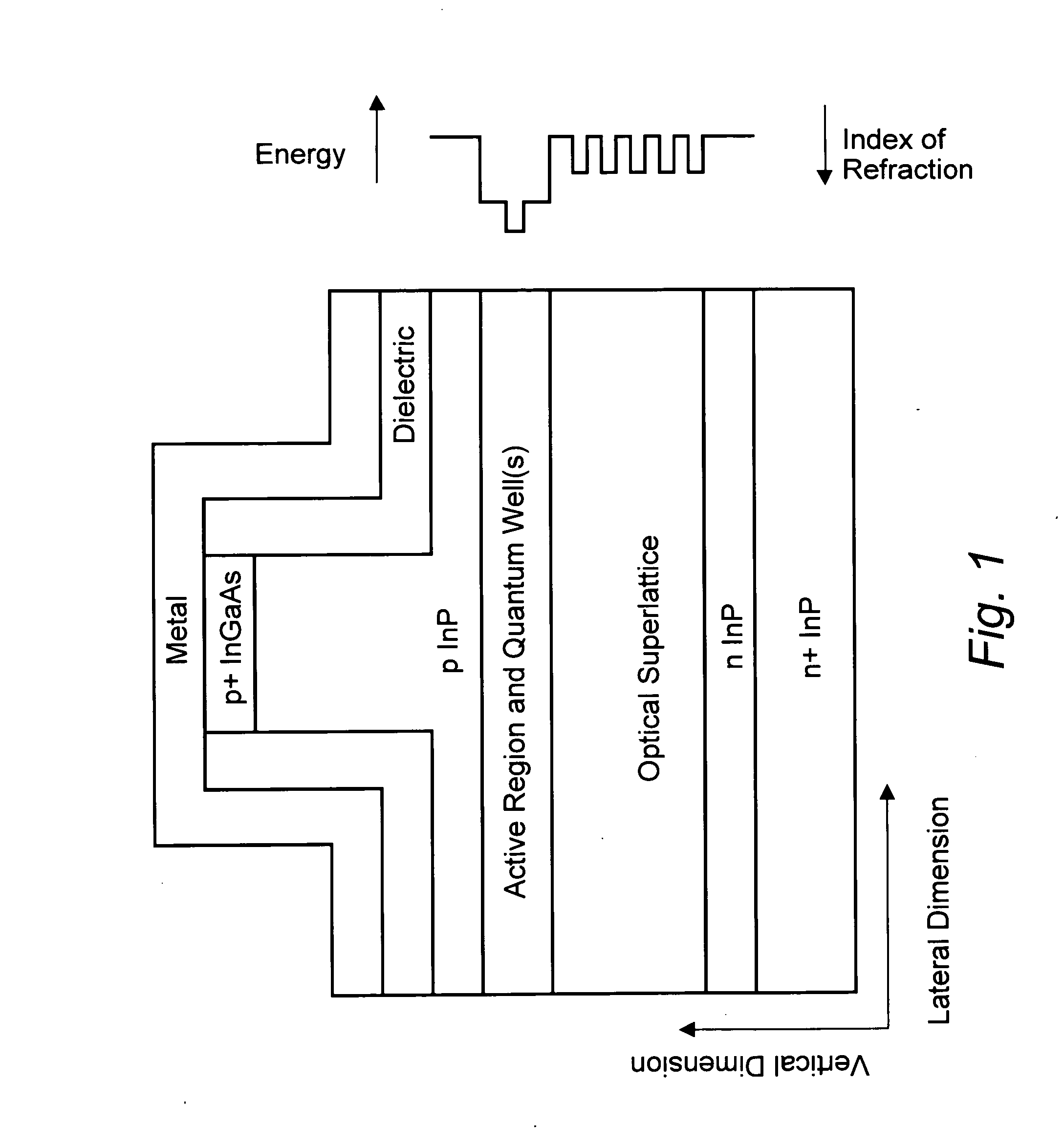
[0035] FIG. 1 shows the basic layout, i.e. the cross section of the essential parts, of a semiconductor laser diode according to the invention, together with the distribution of the associated refraction index on the right. Starting from the bottom of the structure shown in FIG. 1, the n+InP layer represents the InP substrate for the epitaxial growth of the laser structure, followed by an n InP layer, both known from the prior art. On this lower cladding layer, the optical superlattice is located, followed by the laser's active region with a gain region and a waveguide. Preferably the optical superlattice terminates towards the active region with a material with low index of refraction and therefor high bandgap. Most preferably the material with low index of refraction consists of InP. On top of the active region, another cladding layer, here of p InP is situated, forming the laser ridge with a narrow p+InGaAs layer on top of the ridge. The whole structure carries a metallization on...


PUM


Abstract

The invention relates to high power semiconductor diode lasers of the type commonly used in opto-electronics, mostly as so-called pump lasers for fiber amplifiers in the field of optical communication, e.g. for an erbium-doped fiber amplifier (EDFA) or a Raman amplifier. Such a laser, having a single cavity and working in single transverse mode, is improved by placing a multilayer large optical superlattice structure (LOSL) into at least one of the provided cladding layers. This LOSL provides for a significantly improved shape of the exit beam allowing an efficient high power coupling into the fiber of an opto-electronic network.

Description

[0001] The invention relates to high power semiconductor diode lasers of the type commonly used in opto-electronics, mostly as so-called pump lasers for fiber amplifiers in the field of optical communication, e.g. for an erbium-doped fiber amplifier (EDFA) or a Raman amplifier. Such lasers usually have a single cavity and work in single lateral and vertical mode. They provide a narrow-bandwidth optical radiation with a high power output in a given frequency band. In particular, the invention relates to such a laser working at wavelengths of more than 1100 nm.BACKGROUND AND PRIOR ART[0002] Semiconductor lasers of the type mentioned above have, for example, become important components in the technology of optical communication, particularly because such lasers can be used for amplifying optical signals immediately by optical means. This allows to design all-optical fiber communication systems, avoiding any complicated conversion of the signals to be transmitted which improves speed as...

Claims


Application Information

Patent Timeline
Patent Type & Authority Applications(United States)
IPC IPC(8): H01S5/00H01S5/20
CPCH01S5/20H01S2301/18H01S5/3213H01S5/3216H01S2301/166H01S5/2031
Inventor LICHTENSTEIN, NORBERTFILY, ARNAUD CHRISTIANREID, BERTOIT
Owner LUMENTUM TECH UK LTD
Why Eureka
Try Eureka