Plasma processing apparatus

a technology of processing apparatus and plasma, which is applied in the direction of coating, chemical vapor deposition coating, electric discharge tube, etc., can solve the problems of large damage to a device, inability to achieve high-speed high-performance processes, and become difficult to satisfy the demands of semiconductors

Inactive Publication Date: 2004-11-11
TOKYO ELECTRON LTD
View PDF21 Cites 166 Cited by
  • Summary
  • Abstract
  • Description
  • Claims
  • Application Information

AI Technical Summary

Benefits of technology

0012] It is a general object of the present invention to provide an improved and ...

Problems solved by technology

These plasma apparatuses have several essential problems in that a large damage is given to a device and a high-performance process at a high-speed cannot be achieved.
Accordingly, it has become difficult to satisfy demands of semiconductors and liquid crystal displays to have a high-performance and high-throughput
However, these conventional microwave plasma apparatuses have a problem in that a substance, which is produced by dissociation and combination of a process gas due to the plasma, adheres onto a surface of the dielectric material separation wall or the shower plate.
Accordingly, the plasma excitation power is decreased due to adhesion of the substance onto the surface of the dielectric material separation wall or the dielectric material shower plate, which reduces the plasma density and deteriorates stability of the plasma.
In order to eliminate such a problem, it is necessary to frequently perform a chamber cleaning and maintenance so as to remove the adhered film, which significantly decreases the throughput.
However, in the conventional microwave plasma apparatus, since the opposing surface of the substrate is covered by a dielectric material in its entirety, the area of the grounded part to which the plasma contacts cannot be large.
Accordingly, it is difficult to apply to an reactive ion etching such as a process in which a high energy ions must be bombarded to a substrate surface.
However, if the organic molecules are decomposed, a large amount of carbon impurity atoms are mixed into the ...

Method used


Image

  • Plasma processing apparatus
  • Plasma processing apparatus
  • Plasma processing apparatus

Examples


embodiment 2

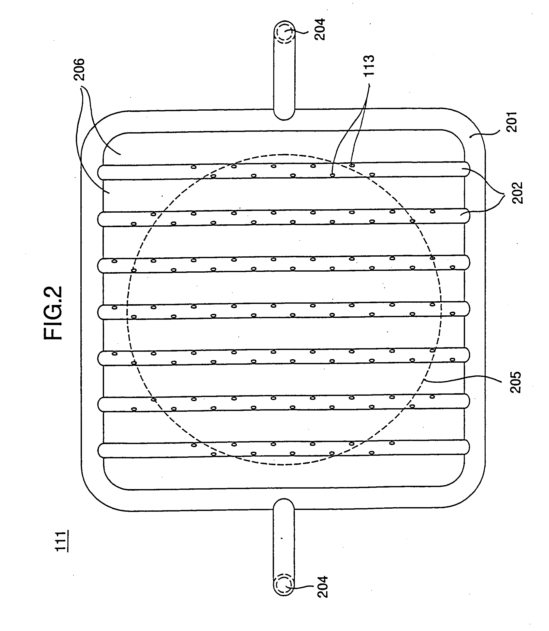
[0074] A description will now be given, with reference to FIG. 11 and FIG. 12, of a plasma processing apparatus according to a second embodiment of the present invention. FIG. 11 is a plan view of a lattice-like shower plate 600 provided in the plasma processing apparatus according to the second embodiment of the present invention viewed from a side of a substrate. FIG. 12 is a cross-sectional view taken along a line XII-XII of FIG. 11. The plasma processing apparatus according to the second embodiment of the present invention is the same as the plasma processing apparatus according to the first embodiment of the present invention shown in FIG. 1 except for the lattice-like shower plate 600 shown in FIG. 11, and descriptions thereof will be omitted.

[0075] As shown in FIG. 11, the lattice-like shower plate 600 comprises a main pipe 601, branch pipes 602, process gas discharge parts 603 (hatched portions) and lattice-like shower plate gas supply ports 604. As shown in FIG. 12, each of...

embodiment 3

[0079] A description will now be given, with reference to FIG. 13 and FIG. 14, of a plasma processing apparatus according to a third embodiment of the present invention. FIG. 13 is a plan view of a lattice-like shower plate 700 provided in the plasma processing apparatus according to the third embodiment of the present invention viewed from a side of a substrate. FIG. 14 is a cross-sectional view taken along a line XIV-XIV of FIG. 13. The plasma processing apparatus according to the third embodiment of the present invention is the same as the plasma processing apparatus according to the first embodiment of the present invention shown in FIG. 1 except for the lattice-like shower plate 700 shown in FIG. 13, and descriptions thereof will be omitted.

[0080] The lattice-like shower plate 700 shown in FIG. 13 comprises gas introducing passages 701, process gas discharging holes 702, lattice-like shower plate gas supply ports 703, a lattice-like shower plate body 705 and a lattice-like show...

embodiment 4

[0083] FIG. 15 is a cross-sectional view of a plasma processing apparatus according to a fourth embodiment of the present invention. The plasma processing apparatus according o the fourth embodiment of the present invention comprises a vacuum chamber 801, a dielectric material separation wall 802, dielectric material shower plates 803, a gap 804, a shower plate fixing jig 805, plasma excitation gas supply ports 806, plasma excitation gas discharge holes 807, microwave guides 808, a lattice-like shower plate 809, process gas supply ports 810, process gas discharge holes 811, a stage 813 and an exhaust port 814. A substrate 812 to be processed by plasma is placed on the stage 813.

[0084] In the present embodiment, the vacuum chamber is formed of aluminum; the dielectric material separation wall 802 is formed of aluminum oxide; the dielectric material shower plates 803 are formed of aluminum nitride; and the shower plate fixing jig 805 is formed of aluminum. The lattice-like shower plat...


PUM

PropertyMeasurementUnit
Thicknessaaaaaaaaaa
Distanceaaaaaaaaaa
Wavelengthaaaaaaaaaa

Abstract

In a microwave plasma processing apparatus, a metal made lattice-like shower plate 111 is provided between a dielectric material shower plate 103, and a plasma excitation gas mainly an inert gas and a process gas are discharged form different locations. High energy ions can be incident on a surface of the substrate 114 by grounding the lattice-like shower plate. The thickness of each of the dielectric material separation wall 102 and the dielectric material at a microwave introducing part is optimized so as to maximize the plasma excitation efficiency, and, at the same time, the distance between the slot antenna 110 and the dielectric material separation wall 102 and a thickness of the dielectric material shower plate 103 are optimized so as to be capable of supplying a microwave having a large power.

Description

[0001] The present invention relates to plasma processing apparatuses and, more particularly, to a plasma processing apparatus which is capable of performing a high performance plasma process and has a high electric-power-efficiency and a long maintenance period.[0002] In recent years, in order to realize semiconductors and liquid crystal displays having a high-performance and high-throughput, a plasma process has become indispensable for manufacturing these products. Although there are various methods for plasma excitation, a parallel plate type RF plasma excitation apparatus or a inductive coupling type plasma apparatus has been used to manufacture semiconductors or liquid crystal displays. These plasma apparatuses have several essential problems in that a large damage is given to a device and a high-performance process at a high-speed cannot be achieved. Accordingly, it has become difficult to satisfy demands of semiconductors and liquid crystal displays to have a high-performanc...

Claims


Application Information

Patent Timeline
IPC IPC(8): C23C16/24C23C16/34C23C16/44C23C16/455C23C16/511H01J37/32
CPCC23C16/24C23C16/345C23C16/45565C23C16/45578C23C16/511H01J37/32192H01J37/3244
Inventor OHMIHIRAYAMA, MASAKI
Owner TOKYO ELECTRON LTD
Why Eureka
Try Eureka