Polishing pad and method of polishing a semiconductor wafer

Inactive Publication Date: 2004-11-11
JSR CORPORATIOON
View PDF8 Cites 38 Cited by
  • Summary
  • Abstract
  • Description
  • Claims
  • Application Information

AI Technical Summary

Problems solved by technology

Therefore, it is extremely inefficient to obtain the polishing time from these.
This polishing pad has a problem that optical end-point detection may become unsatisfactory due to a leak of slurry from the gap between the window member and the polishing pad substrate because the window member becomes loose during polishing.
However, it involves the following problems: (1) the curing of the adhesive takes long, thereby reducing the production yield, and (2) the window member is distorted by the swelling of the adhesive at the time of curing, whereby part of the window member may project from the surface of the polishing pad substrate and accordingly, a polishing pad having a smooth surface may not be obtained.
Meanwhile, when rubber cement or a commonly used adhesive such as an epoxy-based adhesive is used, part of the adhesive may be solidified while it overflows into the polishing surface of the polishing pad or part of the adhesive solidified during polishing may fall off as a fragment, thereby scratching the surface to be polished.
When the average particle diameter is larger than 500 .mu.m, the formed pores become too large, whereby the mechanical strength and polishing rate of the obtain

Method used


Image

  • Polishing pad and method of polishing a semiconductor wafer
  • Polishing pad and method of polishing a semiconductor wafer
  • Polishing pad and method of polishing a semiconductor wafer

Examples


example 1

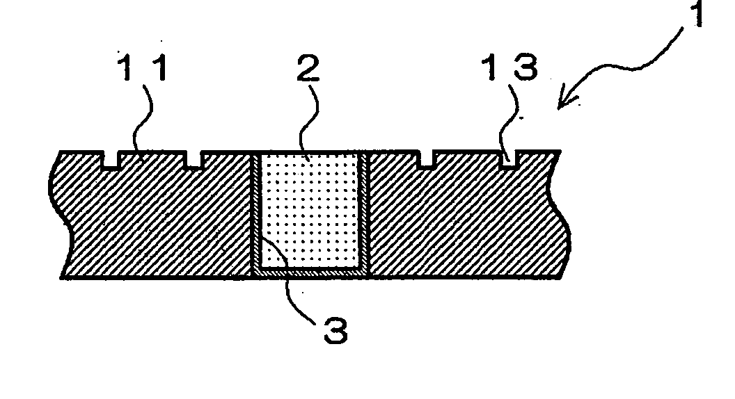
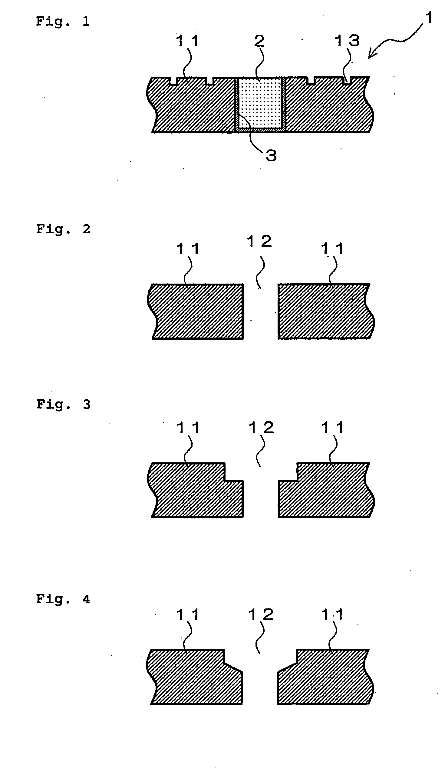
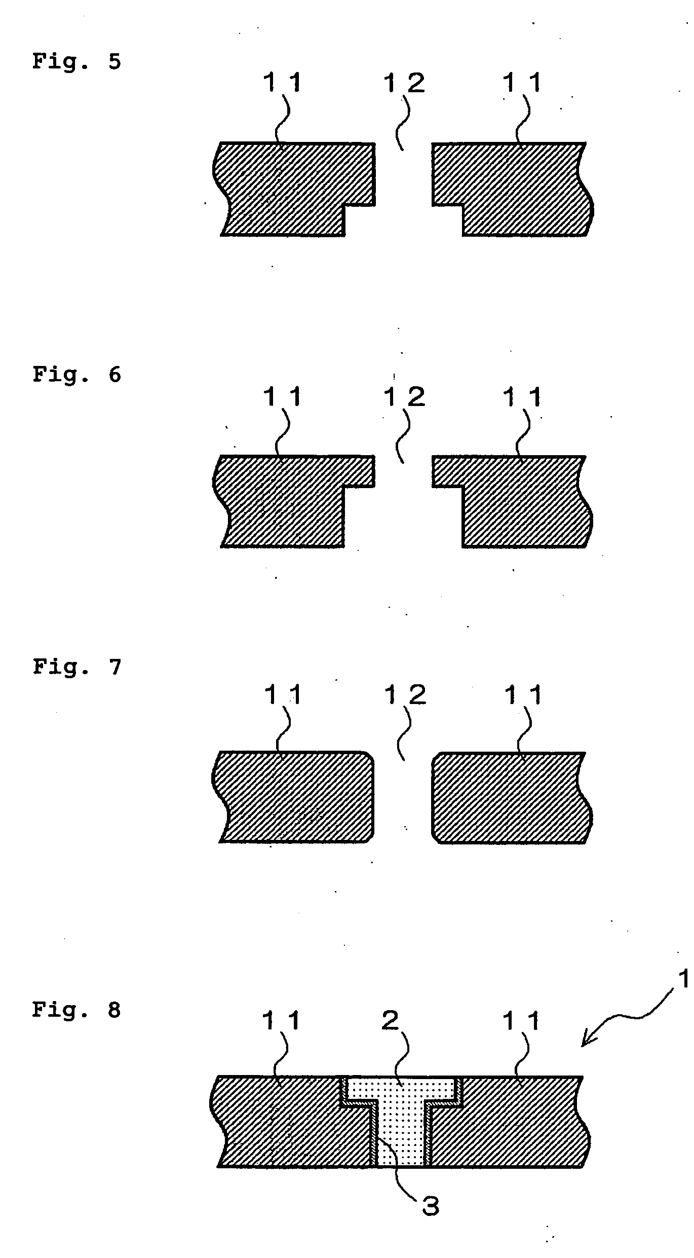
[0159] The polishing substrate 11 obtained in (2) above was set on a testing bench in such a manner that the surface (polishing surface) having the grooves 13 of the polishing substrate 11 faced down, and the light transmitting member 2 obtained in (1) above was inserted into the through hole. Thereafter, 1 ml of a photocurable adhesive essentially composed of a polyurethane acrylate and an ethylenically unsaturated monomer (Desolite Z8007 having a viscosity at 25.degree. C. of 8,000 mPa.s, manufactured by Japan Fine Coatings Co., Ltd.) was applied to the light transmitting member 2 uniformly, filled in the gap between the outer wall of the light transmitting member 2 and the inner wall of the through hole to ensure that it did not overflow into the polishing surface facing down and cured by exposure to 5,000 J / m.sup.2 of light from a halogen lamp to form an adhesive layer 3, thereby obtaining the polishing pad 1 (I) shown in FIG. 1 and FIG. 20.

[0160] The adhesive used herein had an...

example 2

[0165] The polishing pad (I) obtained in Example 1 was mounted on the platen of a polishing machine equipped with an optical end-point detection device to polish a copper film wafer while slurry containing abrasive particles was supplied at a flow rate of 100 ml / min and a platen revolution of 50 rpm. As a result, the polishing rate was 7,200 .ANG. / min. The slurry did not leak to the non-polishing surface of the polishing pad (I) from the gap between the outer wall of the light transmitting member and the inner wall of the through hole during polishing. No scratch was observed on the polished surface of the copper film wafer when seen through an optical microscope (MX50 of Olympus Co., Ltd.) at a magnification of .times.200 in a dark field mode.


PUM


Abstract

A polishing pad, a polishing laminated pad and a semiconductor wafer polishing method all of which prevent a leak of slurry from the gap between a polishing substrate and a reduction in polishing efficiency caused by a scratched and a window member and enable the optical detection of the polishing end point to be carried out efficiently. The polishing pad comprises a polishing substrate having a through hole extending from the front side to the rear side and a light transmitting member arranged in the through hole, and the outer wall of the above light transmitting member and the inner wall of the though hole opposite to the outer wall are bonded together with a photocurable adhesive such as a polyurethane(meth)acrylate to fix the above light transmitting member in the through hole.

Description

[0001] The present invention relates to a polishing pad and a method of polishing a semiconductor wafer. More specifically, it relates to a polishing pad comprising a window member for optical end-point detection, which prevents a leak of slurry from the gap between a polishing pad substrate and the window member and which enables the optical detection of the polishing end point to be carried out efficiently without a reduction in polishing efficiency caused by a scratched surface to be polished and to a method of polishing a semiconductor wafer with the polishing pad.DESCRIPTION OF THE PRIOR ART[0002] In the polishing of a semiconductor wafer, after the purpose of polishing is accomplished, the determination of the polishing end point for terminating polishing can be made based on a time obtained empirically. However, various materials are used to form surfaces to be polished and the polishing time differs by each material. It is conceivable that the material forming the surface to...

Claims


Application Information

Patent Timeline
IPC IPC(8): B24B37/20H01L21/304B24D13/14
CPCB24B37/205A61J11/007A61J11/0035A61J11/006
Inventor AOI, HIROMISHIHO, HIROSHIHASEGAWA, KOUKAWAHASHI, NOBUO
Owner JSR CORPORATIOON
Why Eureka
Try Eureka