

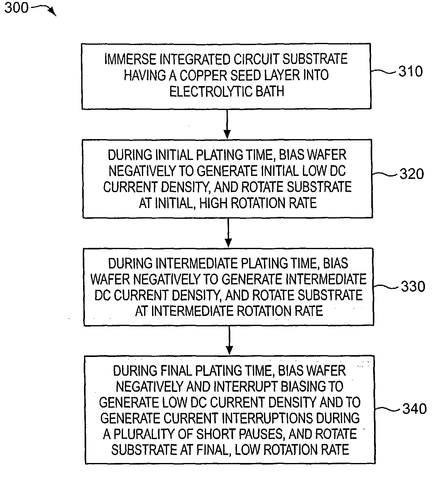
Electroplating using DC current interruption and variable rotation rate
a technology of dc current interruption and variable rotation rate, applied in the direction of transportation and packaging, other domestic articles, coatings, etc., can solve the problems of affecting the ability to accurately identify device-killing defects, affecting the accuracy of device-killing defects, and difficulty in measuring defects on copper deposits
- Summary
- Abstract
- Description
- Claims
- Application Information
AI Technical Summary
Problems solved by technology
Method used
Image

Examples
example 2
[0050] A copper layer having a thickness of 0.7 .mu.m, or 700 nm, was electroplated on a series of wafers using Waveform 2 as implemented in Example 1 above, but the rotation rate of the wafer was varied during electroplating. During the intermediate plating time of Waveform 2, each substrate wafer was rotated at a speed selected from 10, 25, 50, and 75 rpm. During the final 3rd-step plating time, each substrate wafer was rotated at a speed selected from 10, 25, and 50 rpm. Defects were measured as described in Example 1. FIG. 5 shows a graph in which measured defect count is plotted as a function of intermediate 2nd-step rotation rate. The results show that the 2nd-step rotation rate did not have a substantial effect on protrusion-defect counts. In contrast, there is a correlation between 3rd-step rotation rate and defect count. A copper layer fabricated using a final 3rd-step rotation rate of 10 rpm generally has a lower defect count than copper layers fabricating using a final 3r...
example 3
[0051] A copper layer having a thickness of 0.7 .mu.m, or 700 nm, was electroplated on a series of wafers as in Example 1, but using various combinations of DC current waveforms and varied rotation rates in accordance with the invention. Defects were measured as described in Example 1.
[0052] FIG. 6 contains a graph in which defect count is plotted as a function of a particular combination of waveform and 2nd-step and 3rd-step rotation rates. The first set of bars plotted at the left of the graph of FIG. 6 represents defect counts in copper layers fabricating using the conventional POR of Table 1 and a standard rotation rate of 125 rpm. The second set of bars from the left represents defect counts of copper layers formed using Waveform 2 of Table 1 in accordance with the invention, without varying the standard rotation rate of 125 rpm. The third set of bars from the left represents defect counts of copper layers formed using Waveform 1 of Table 1, in accordance with the invention, wi...
example 4
[0053] A long-term marathon test was conducted using the apparatus and plating solution of Example 1 to establish the impact of process modifications on long-term plating tool behavior and film properties. Conventional three-step and four-step current waveforms were used with a constant rotation rate of 125 rpm. The conventional three-step waveform corresponded to the Waveform POR of Table 1, except the first current step was conducted at 0.5 amps for 22 seconds. The conventional four-step waveform had a first current step of 0.5 amps for 22 seconds, a second current step of 3 amps for 30 seconds, a third current step of 7.5 amps for 20 seconds, and a fourth current step of 15 amps for 35 seconds. Also, a conventional three-step waveform was used, but the rotation rate was decreased from 125 rpm to 18 rpm during the final third step. Further, a three-step waveform corresponding to Waveform 1 of Table 1 with interruptions of 50 msec in accordance with the invention and including decr...
PUM
| Property | Measurement | Unit |
|---|---|---|
| current density | aaaaa | aaaaa |
| current density | aaaaa | aaaaa |
| current density | aaaaa | aaaaa |
Abstract
Description
Claims
Application Information