
Double HBT base metal micro-bridge

a technology of base metal and micro-bridges, applied in the direction of basic electric elements, electrical apparatus, semiconductor devices, etc., can solve the problem of reducing the base-collector capacitance, and achieve the effect of reducing the base mesa area, facilitating mitigation of base-collector capacitance, and reducing the base-collector capacitan

Inactive Publication Date: 2004-12-02
NORTHROP GRUMMAN SYST CORP
View PDF11 Cites 9 Cited by
  • Summary
  • Abstract
  • Description
  • Claims
  • Application Information

AI Technical Summary

Benefits of technology

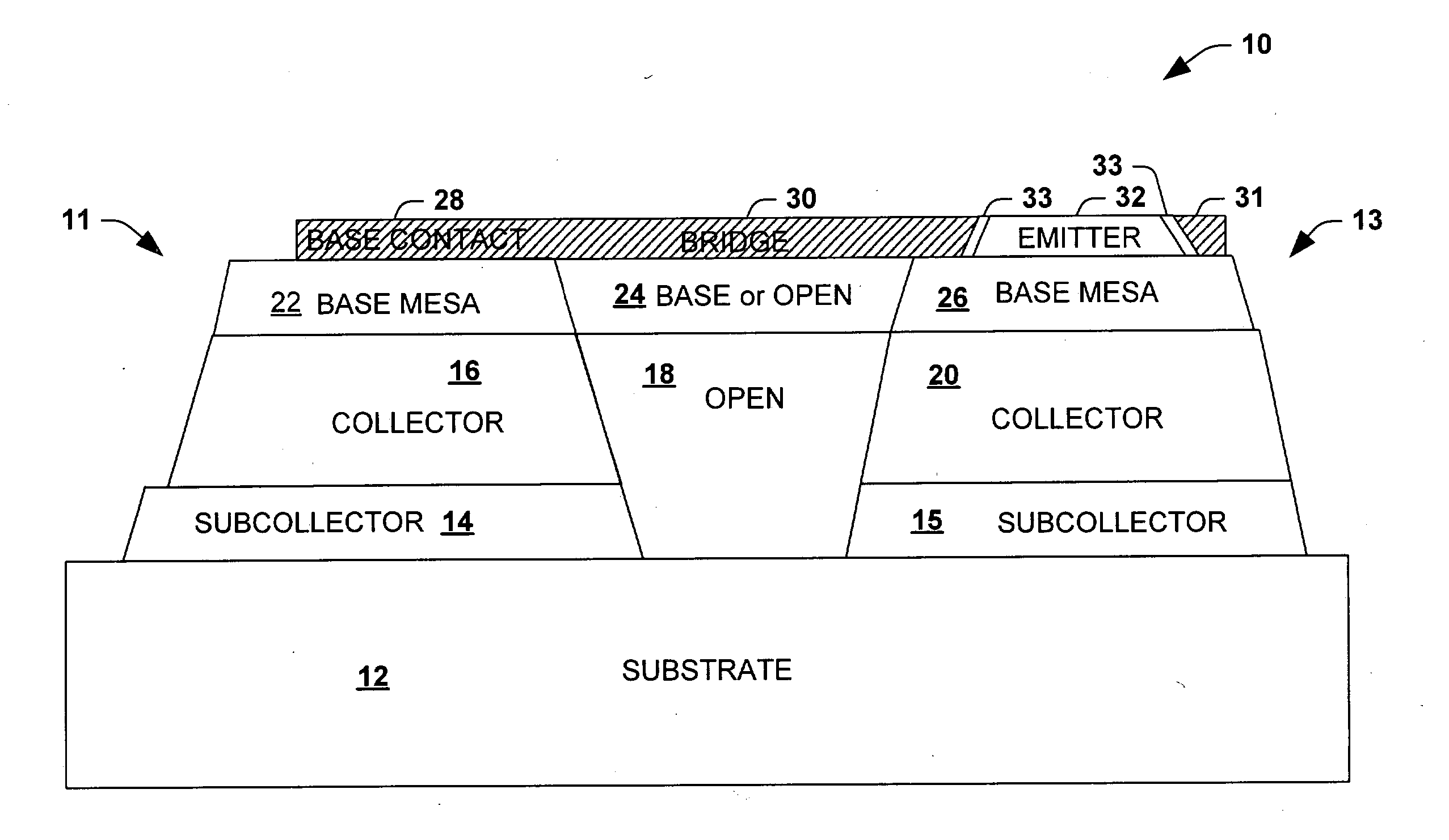
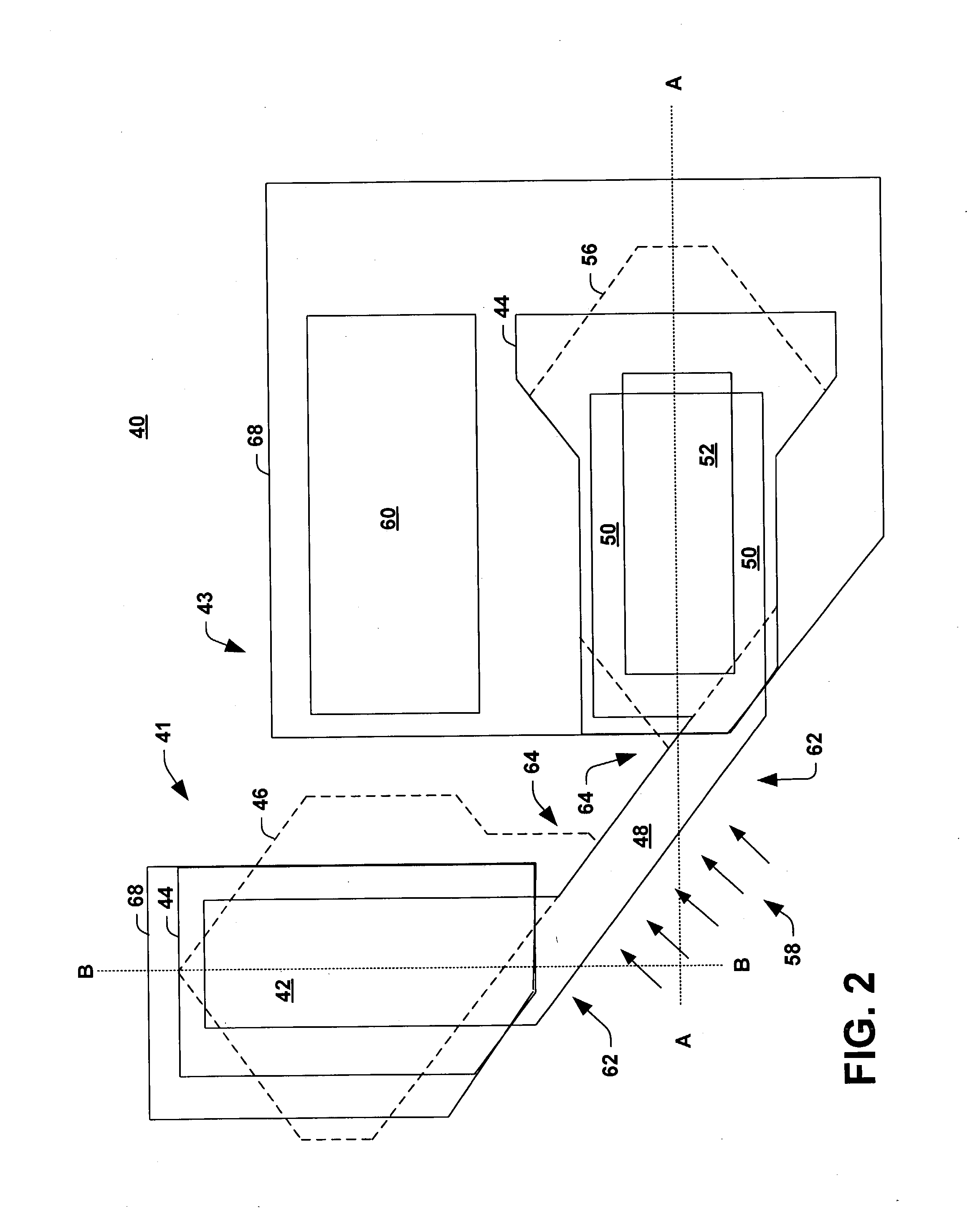
[0007] The present invention relates to a HBT device structure which facilitates mitigation of base-collector capacitance and a method for making the same. The HBT device structure of the present invention employs a phosphorous based collector material. During removal of the phosphorous based collector material, for example, using a wet etch, only facets or geometric surfaces that are part of a convex side of the HBT, and are oriented at about a .+-.45.degree. (010 or 001 direction) or about a .+-.135.degree. (00{overscore (1)} or 0{overscore (1)}0 direction) from the major flat of the wafer will be undercut (major flat is in the 001 crystal plane). The base-collector capacitance is decreased by reducing the base mesa area and fabricating a base connecting bridge or micro-bridge that electrically connects a base contact to the base mesa. The base connecting bridge is positioned along a 45.degree. angle to a major flat of the wafer. During collector removal, the base layer is undercut forming the connecting bridge, successfully removing the collector and sub-collector material below the bridge. The removal of collector and sub-collector material will reduce the base-collector junction area, and therefore reduce the base-collector junction capacitance.
[0008] Additionally, a base undercut cantilever base contact structure further reduces the base-collector capacitance. The base undercut cantilever base contact structure is provided by aligning the orientation of the intrinsic HBT portion and base contact portions along a 45.degree. angle to the major flat. Therefore, undercutting portions of the collector and subcollector that have a convex geometric surface under the base mesas during the etching process a cantilever base contact structure.

Problems solved by technology

Additionally, a base undercut cantilever base contact structure further reduces the base-collector capacitance.

Method used


Image

  • Double HBT base metal micro-bridge
  • Double HBT base metal micro-bridge
  • Double HBT base metal micro-bridge

Examples


Embodiment Construction

[0028] The present invention relates to a HBT device structure which facilitates mitigation of base-collector capacitance and a method for making the same. The HBT device of the present invention exhibits faster performance at higher frequencies than many conventional HBT devices. The HBT device of the present invention employs a phosphorous (e.g., Indium Phosphide (InP), Indium Gallium Phosphide (InGaP)) based collector material. During removal of the phosphorous based collector material, for example, by using a wet etch, only facets that are part of a convex side of the HBT, and are oriented about a .+-.45.degree. (010 or 001 direction) or about a .+-.135.degree. (00{overscore (1)} or 0{overscore (1)}0 direction) from the major flat of the wafer will be undercut (major flat is in the 00{overscore (1)} crystal plane). The base-collector capacitance is decreased by fabricating a base micro-bridge on an InP-based HBT or double HBT (DHBT) by positioning the base micro-bridge along abo...


PUM


Abstract

A heterojunction bipolar transistor (HBT) device structure is provided which facilitates the reduction of the base-collector capacitance and a method for making the same. The base-collector capacitance is decreased by fabricating a base micro-bridge connecting a base contact to a base mesa on the HBT. The base micro-bridge is oriented along about one of 001, 010, 00{overscore (1, and 0{overscore (10 direction to a major flat of the wafer. The HBT device employs a phosphorous based collector material. During removal of the phosphorous based collector material, the base layer is undercut forming the micro-bridge, successfully removing the collector and sub-collector material below the bridge due to the orientation of the micro-bridge. The removal of collector and sub-collector material reduces the base-collector junction area, and therefore reduce the base-collector junction capacitance.

Description

[0001] The present invention relates generally to electrical circuits, and more particularly to fabrication of heterojunction bipolar transistors.[0002] Heterojunction bipolar transistors (HBTs) are widely used in high speed and high frequency applications. The heterojunction bipolar transistor (HBT) offers much higher speeds of operation than the more prevalent metal-oxide-semiconductor field-effect transistors (MOSFETS) or even conventional homojunction bipolar transistors, such as npn or pnp silicon transistors. The HBT offers an alternative technology to metal semiconductor field effect transistors (MESFETs) and high electron mobility transistors (HEMTs) when a high degree of linearity is desirable. The use of different materials of differing bandgaps for the collector, base and emitter provides for * additional design flexibility. The HBT is a layered structure that includes a semiconductor substrate, a subcollector, a collector, a base and an emitter stacked one on top the oth...

Claims


Application Information

Patent Timeline
Patent Type & Authority Applications(United States)
IPC IPC(8): H01L29/417H01L21/331H01L29/423H01L29/737
CPCH01L29/42304H01L29/66318H01L29/7371H01L29/20
Inventor SAWDAI, DONALD JAMESLESLIE, GREGORY SCOTTGUTIERREZ-AITKEN, AUGUSTO
Owner NORTHROP GRUMMAN SYST CORP
Learn More