Plasma processing apparatus and plasma processing method

Inactive Publication Date: 2005-01-06
ADVANCED LCD TECH DEVMENT CENT
View PDF15 Cites 16 Cited by
  • Summary
  • Abstract
  • Description
  • Claims
  • Application Information

AI Technical Summary

Benefits of technology

The particular construction described above makes it possible to provide a plasma processing apparatus, which permits processing a substrate having a large surface area, which is small in its footprint, and which permits forming a plasma having a uniform plasma density.
It is desirable for the plasma processing apparatus of the present invention to be constructed to permit the electromagn

Problems solved by technology

Also, a DC magnetic field is required for the plasma excitation in the ECR plasma processing apparatus so as to give rise to the problem that it is difficult to apply a plasma processing to a large area.
In recent years, the plasma processing apparatus used for manufacturing a semiconductor device or a liquid crystal display device is being rendered bulky with increase in the substrate size.
Each of the known plasma processing apparatuses pointed out above gives rise to a serious problem as pointed out below.
This gives rise to the problem that the plasma tends to be concentrated in the vicinity of the slot through which the microwave is emitted.
The difficulty is rendered more serious in the case where the plasma pressure is high.
It follows that it is difficult to use the plasma processing apparatus of the particular construction for application of a plasma processing using as the raw material the gases easily forming a nega

Method used


Image

  • Plasma processing apparatus and plasma processing method
  • Plasma processing apparatus and plasma processing method
  • Plasma processing apparatus and plasma processing method

Examples


Example

FIRST EMBODIMENT

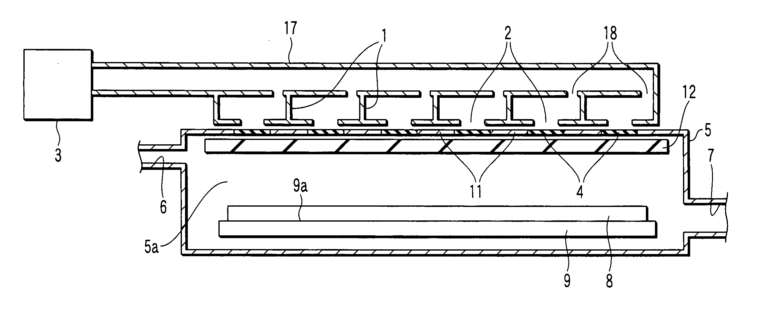
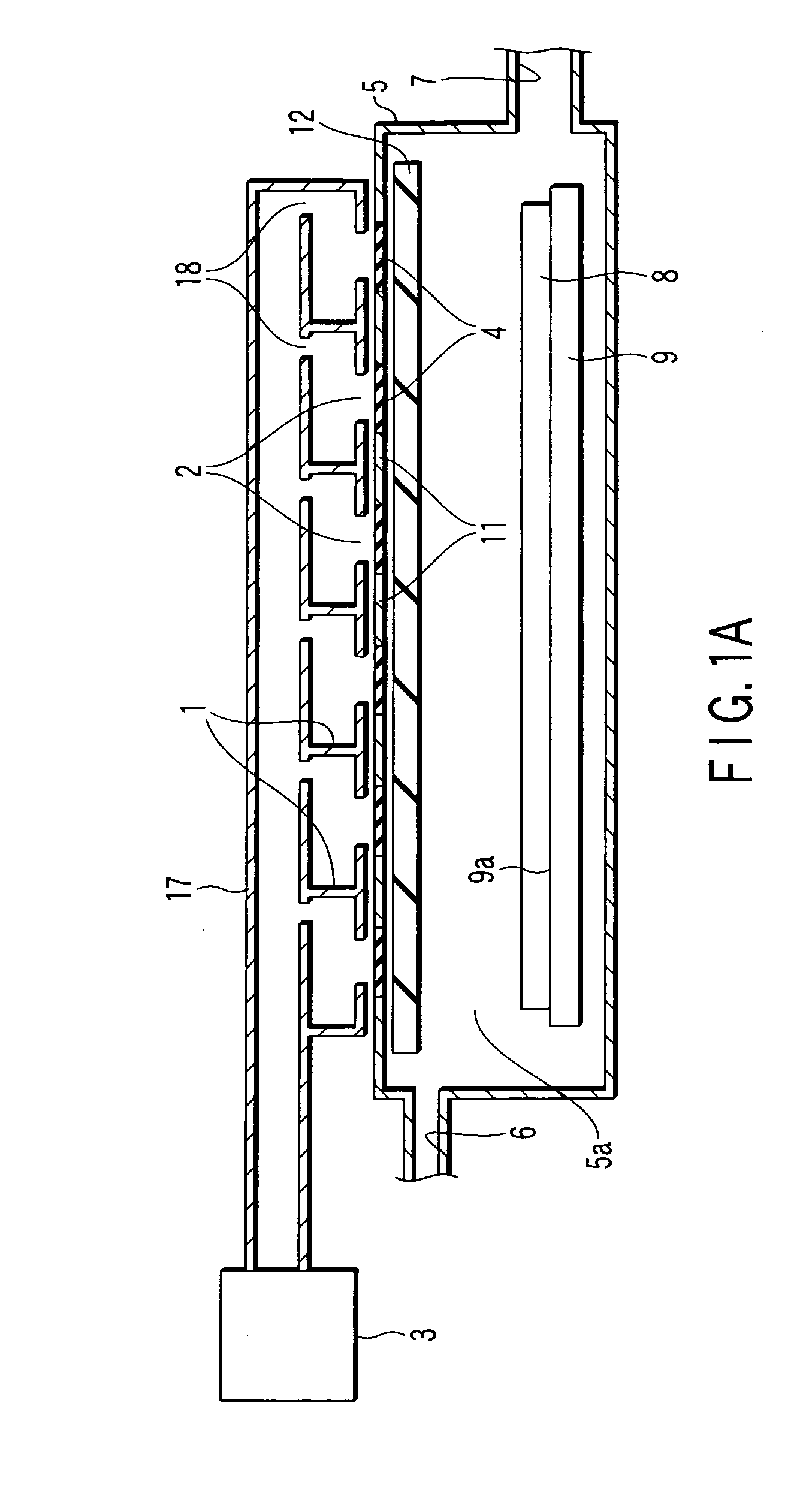
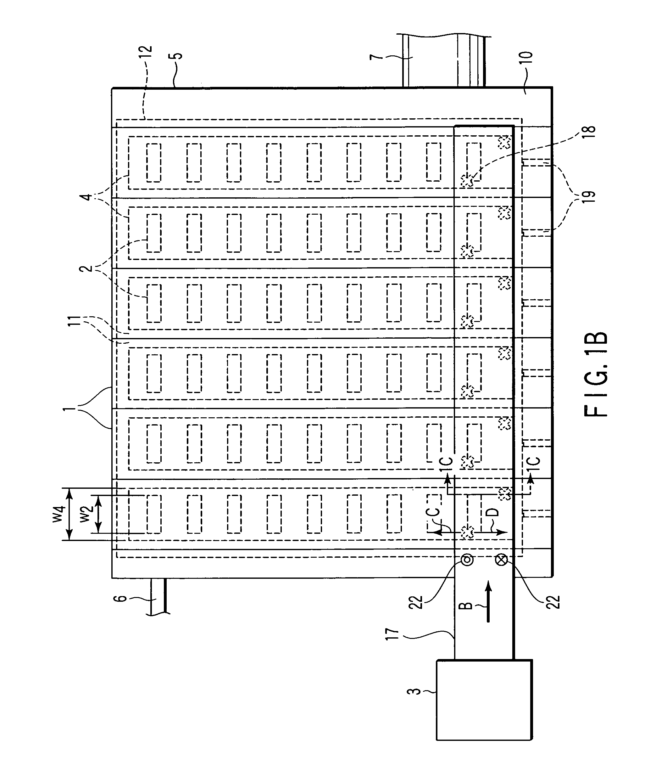
FIG. 1A is a cross sectional view schematically showing the construction of a plasma processing apparatus according to a first embodiment of the present invention. FIG. 1B is an upper view of the plasma processing apparatus shown in FIG. 1A. FIG. 1C is a cross sectional view along the line 1C-1C shown in FIG. 1B. A waveguide portion for distributing the electromagnetic wave and a waveguide are partly shown in a magnified fashion in FIG. 1C. Further, FIG. 1D schematically shows the propagating direction and the rotating direction of the circular polarization of the electromagnetic wave utilized in the plasma processing apparatus shown in FIG. 1A.

A reference numeral 1 shown in the drawing denotes a plurality of waveguides for radiating an electro-magnetic wave to a vacuum vessel 5 referred to herein later. For example, a rectangular waveguide, i.e., a waveguide having a rectangular cross section, can be used as the waveguide 1. These waveguides 1 are formed to have ...

Example

SECOND EMBODIMENT

FIG. 2A is a cross sectional view showing the construction of a plasma processing apparatus according to a second embodiment of the present invention, and FIG. 2B is an upper view of the plasma processing apparatus shown in FIG. 2A.

In the plasma processing apparatus according to the first embodiment of the present invention, a plurality of rectangular waveguides 1 are arranged in contact with each other. In the plasma processing apparatus for the second embodiment of the present invention, however, the width w1 of the rectangular waveguide 1, i.e., the distance in the extending direction of the electromagnetic wave-distributing waveguide portion 17 between the mutually facing inner surfaces, which extend in parallel to each other, of the rectangular waveguide 1 is set at 9 cm, and the distance d1 between the inner surfaces of the adjacent rectangular waveguides 1 is set at 7 cm. It is desirable for the distance d1 noted above to be set such that an electromagneti...

Example

THIRD EMBODIMENT

FIG. 3A is a cross sectional view showing the construction of a plasma processing apparatus according to a third embodiment of the present invention, and FIG. 3B is an upper view of the plasma processing apparatus shown in FIG. 3A.

In the plasma processing apparatus according to the first embodiment of the present invention, the electromagnetic wave-distributing waveguide portion 17 and each of the waveguides 1 extend in directions perpendicular to each other, and the electromagnetic wave-distributing waveguide portion 17 is coupled with each of the waveguides 1 by using the coupling hole section 18 having two cross-shaped holes.

The particular construction is known to the art as the cross-guide coupler. In the plasma processing apparatus according to the third embodiment of the present invention, however, a circular coupling hole 20 is formed in the central portion of the overlapping region between the electromagnetic wave-distributing waveguide portion 17 and ea...


PUM

PropertyMeasurementUnit
Angleaaaaaaaaaa
Frequencyaaaaaaaaaa
Lengthaaaaaaaaaa

Abstract

A plasma processing apparatus includes at least one electromagnetic wave source for generating an electromagnetic wave, an electromagnetic wave-distributing waveguide portion for distributing the electromagnetic wave generated from the electromagnetic wave source, a plurality of waveguides each coupled with the electromagnetic wave-distributing waveguide portion, the waveguides being provided on the same plane, a plurality of slots provided in each of the waveguides, at least one electromagnetic wave radiating window provided to face each slot, and a vacuum vessel in which a plasma is generated by the electromagnetic wave radiated from the electromagnetic wave radiating window. The electromagnetic wave-distributing waveguide portion is provided on the plural waveguides.

Description

CROSS-REFERENCE TO RELATED APPLICATIONS This application is based upon and claims the benefit of priority from prior Japanese Patent Application No. 2003-271007, filed Jul. 4, 2003, the entire contents of which are incorporated herein by reference. BACKGROUND OF THE INVENTION 1. Field of the Invention The present invention relates to a plasma processing apparatus and a plasma processing method, particularly, to a plasma processing apparatus and a plasma processing method suitable for employment for application of a plasma processing to a large angular substrate. 2. Description of the Related Art It is known to the art that a parallel plate type high frequency plasma processing apparatus or an electron cyclotron resonance (ECR) plasma processing apparatus is used for application of a plasma processing such as a film deposition, a surface modification or an etching in the manufacturing process of, for example, a semiconductor device or a liquid crystal display device. In the par...

Claims


Application Information

Patent Timeline
IPC IPC(8): C23C16/00H01L21/3065H01J37/32H05H1/46
CPCH01J37/32229H01J37/32192H01L21/3065H05H1/46
Inventor NAKATA, YUKIHIKOIDE, TETSUYA
Owner ADVANCED LCD TECH DEVMENT CENT
Why Eureka
Try Eureka