Organic thin film transistor comprising multi-layered gate insulator

a thin film transistor and gate insulator technology, applied in transistors, thermoelectric devices, solid-state devices, etc., can solve the problems of unsatisfactory charge mobility, lower charge mobility achieved by n. jackson, and so as to achieve lower driving and threshold voltages, the effect of increasing the charge mobility

Active Publication Date: 2005-01-06
SAMSUNG ELECTRONICS CO LTD
View PDF6 Cites 68 Cited by
  • Summary
  • Abstract
  • Description
  • Claims
  • Application Information

AI Technical Summary

Benefits of technology

The present inventors devoted much effort to meet these demands and found that, when using a multi-layered gate insulator including a first layer of a high K material and a second layer of an insulating polymer being compatible with an organic active layer and positioned directly beneath the organic active layer, the OTFT thus obtained exhibits a higher charge mobility and a lower driving and threshold voltages and its whole preparation can be achieved by a wet process, such as printing or spin coating.
Therefore, a feature of an embodiment of the present invention is to provide an organic thin film transistor comprising a gate electrode, a gate insulating film, an organic active layer and a source / drain electrode, or a gate electrode, a gate insulating film, a source / drain electrode and an organic active layer, sequentially formed on a substrate, wherein the gate insulating film is a multi-layered insulator comprising i) a first layer of a high dielectric material and ii) a second layer of an insulating organic polymer being compatible with the organic active layer and positioned directly under the organic active layer.

Problems solved by technology

But, compared with the amorphous Si TFT, the OTFT exhibits disadvantageously lower charge mobility and higher driving and threshold voltages.
However, the charge mobility achieved by N. Jackson still falls short of the required value, and as well, the OTFT in the prior art requires a driving voltage higher than 100 V and a sub-threshold voltage at least 50 times as high as that of amorphous silicon-TFT.
By using this high k insulator, the driving voltage can be decreased to −5V, but the charge mobility still remains unsatisfactory, lower than 0.6 cm2·V−1·sec−1.
Further, since the process requires high temperatures of 200-400° C., there is a limit in selecting the type of the substrate and as well, it becomes impossible to adopt a common wet process such as simple coating or printing.
U.S. Pat. No. 6,232,157 discloses a method of using polyimide, benzocyclobutene or polyacryl as the organic insulating film, but, the OTFT prepared by the method cannot exhibit device characteristics equal to those of the TFT of inorganic insulator.
However, these patents are inherently related to the inorganic TFT using the inorganic material, such as amorphous or monocrystalline silicon, and thus cannot be applied in the preparation of the organic semiconductor device.
However, satisfactory results have yet to be obtained.

Method used


Image

  • Organic thin film transistor comprising multi-layered gate insulator
  • Organic thin film transistor comprising multi-layered gate insulator
  • Organic thin film transistor comprising multi-layered gate insulator

Examples


example 1

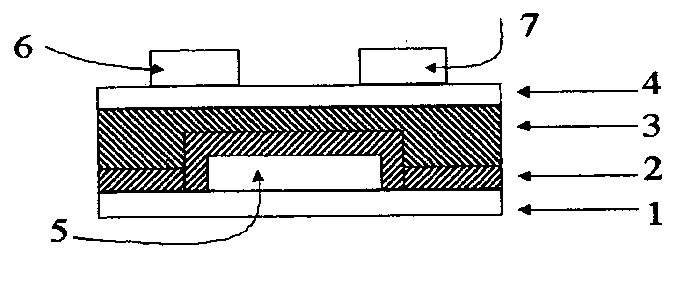
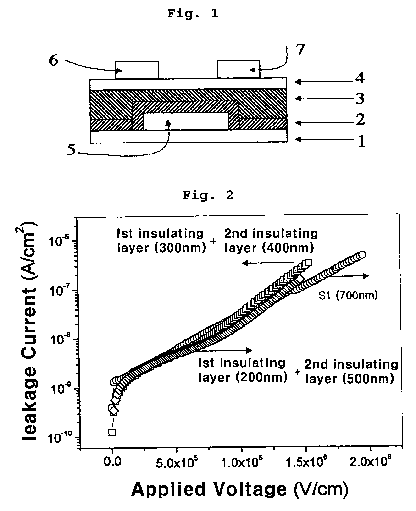
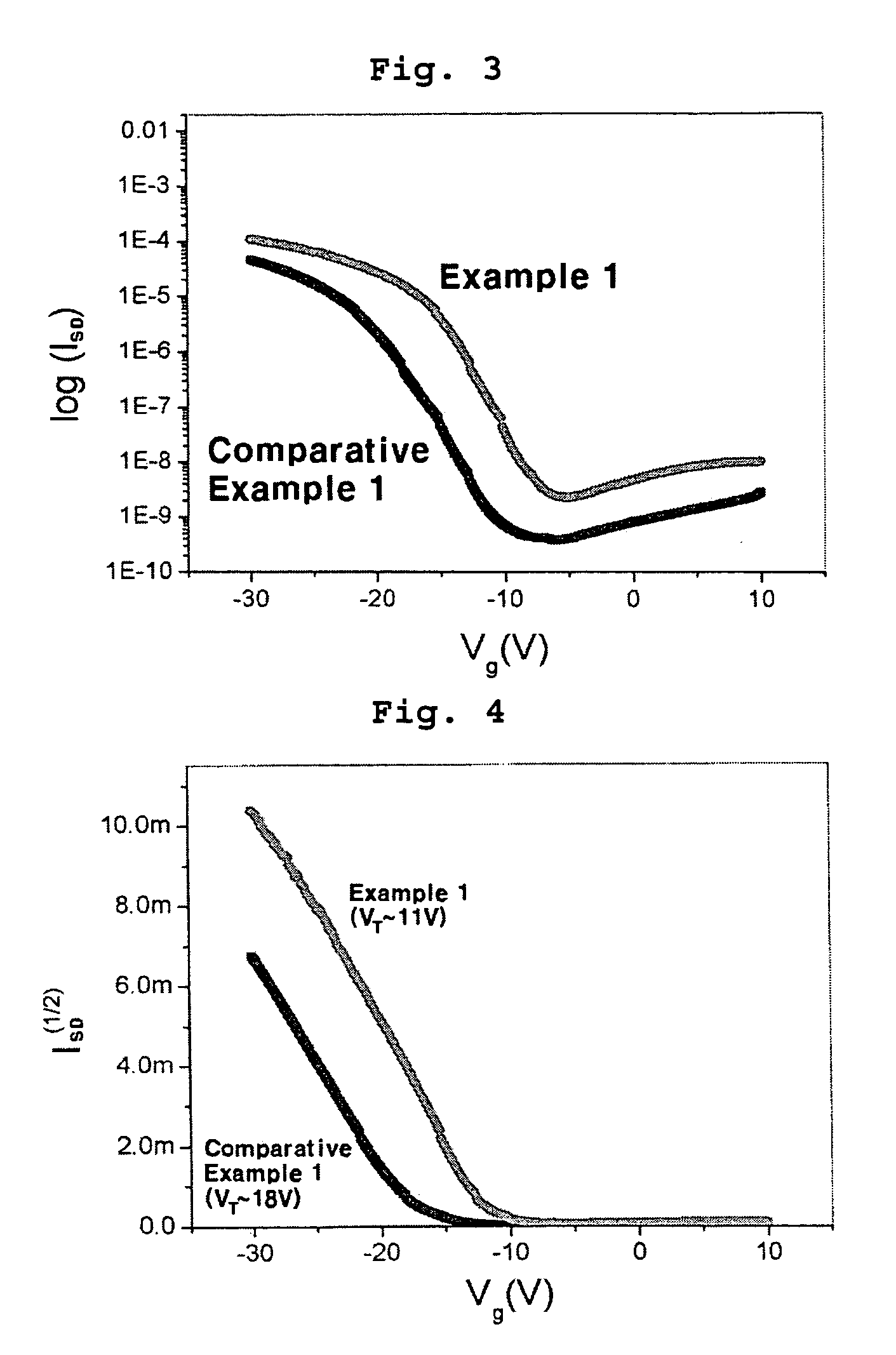
On a glass substrate having a gate electrode made of aluminum, a first insulating layer was formed in the same manner as in Preparative Example 2. A cyclohexanone solution (100 wt %) of a polymer (S1) represented by Formula 3 was prepared, and spin-coated on the first insulating layer to form a 5000 Å thick film, which was then baked at 100° C. for 1 hour in a nitrogen atmosphere, to prepare a two-layered gate insulating film having a total thickness of 700 nm. Then, a 700 Å thick pentacene organic active layer was formed on the gate insulating film by using an OMBD (Organic Molecular Beam Deposition) process, which is performed under 2×10⁻⁶ torr with a deposition rate of 0.3 Å / sec while maintaining a substrate temperature at 80° C. On the active layer thus obtained, a source / drain electrode was formed by a top contact method using a shadow mask having a channel length of 100 μm and a channel width of 1 mm, thereby fabricating an OTFT. For the OTFT thus obtained, a dielectric const...

example 2

An OTFT was prepared in the same manner as in Example 1, with the exception that the first insulating layer was formed using the composition and the solvent under the conditions same as in Preparative Example 3. For the OTFT, a dielectric constant per unit area (C0: nF / unit area), threshold voltage, Ion / Ioff value, and charge mobility were measured in accordance with the same procedures as Example 1. The results are shown in Table 2 below.

example 3

An OTFT was prepared in the same manner as in Example 1, with the exception that a 300 nm-thick first layer and a 400 nm-thick second layer were adopted. For the OTFT, a dielectric constant per unit area (C0: nF / unit area), threshold voltage, Ion / Ioff value, and charge mobility were measured in accordance with the same procedures as Example 1. The results are shown in Table 2 below.


PUM

PropertyMeasurementUnit
dielectric constantaaaaaaaaaa
threshold voltageaaaaaaaaaa
dielectric constantaaaaaaaaaa

Abstract

An organic thin film transistor (OTFT) comprising a gate electrode, a gate insulating film, an organic active layer and a source/drain electrode, or a gate electrode, a gate insulating film, a source/drain electrode and an organic active layer, sequentially formed on a substrate, wherein the gate insulating film is a multi-layered insulator comprising a first layer of a high dielectric material and a second layer of an insulating organic polymer compatible with the organic active layer, the second layer being positioned directly under the organic active layer. The OTFT of the present invention shows low threshold and driving voltages, high charge mobility, and high Ion/Ioff, and it can be prepared by a wet process.

Description

This non-provisional application claims priority under 35 U.S.C. §119(a) from Korean Patent Application No. 2003-44799 filed on Jul. 3, 2003, which is herein incorporated by reference. BACKGROUND OF THE INVENTION 1. Field of the Invention The present invention relates to organic thin film transistors, and in particular, to an organic thin film transistor including a gate electrode, a gate insulating film, an organic active layer and a source / drain electrode, or a gate electrode, a gate insulating film, a source / drain electrode and an organic active layer, sequentially formed on a substrate, wherein the gate insulating film is a multi-layered insulator comprising a first layer of a high dielectric constant (k) material and a second layer of an insulating organic polymer compatible with the organic active layer, the second layer being positioned directly under the organic active layer. 2. Description of the Related Art In recent years, most of thin film transistors (TFT) used for...

Claims


Application Information

Patent Timeline
Patent Type & Authority Applications(United States)
IPC IPC(8): C08F222/40C08F212/14H01L21/312H01L21/316H01L29/786H01L51/05H01L51/30
CPCH01L21/31604H01L21/31691H01L51/0545H01L51/0529H01L51/0537H01L51/0052H01L21/02118H01L21/02194H01L21/02183H01L21/02186H01L21/02197H01L21/02282H01L21/02189H01L21/02205H01L21/02175H10K85/615H10K10/474H10K10/478H10K10/466H01L29/786B82Y30/00
Inventor LEE, SANG YOONPARK, JONG JINLYU, YI YEOLBYUN, YOUNG HUNKOO, BON WONKANG, IN NAM
Owner SAMSUNG ELECTRONICS CO LTD
Why Eureka
Try Eureka