Method for manufacturing gallium nitride group compound semiconductor
a gallium nitride and compound semiconductor technology, applied in the direction of polycrystalline material growth, crystal growth process, radiofrequency control device, etc., can solve the problems of degrading device characteristics improve the crystallinity and reduce the surface density of vertical through-dislocation of the second gallium nitride group compound semiconductor
- Summary
- Abstract
- Description
- Claims
- Application Information
AI Technical Summary
Benefits of technology
Problems solved by technology
Method used
Image
Examples
first embodiment
[0016] (First Embodiment)
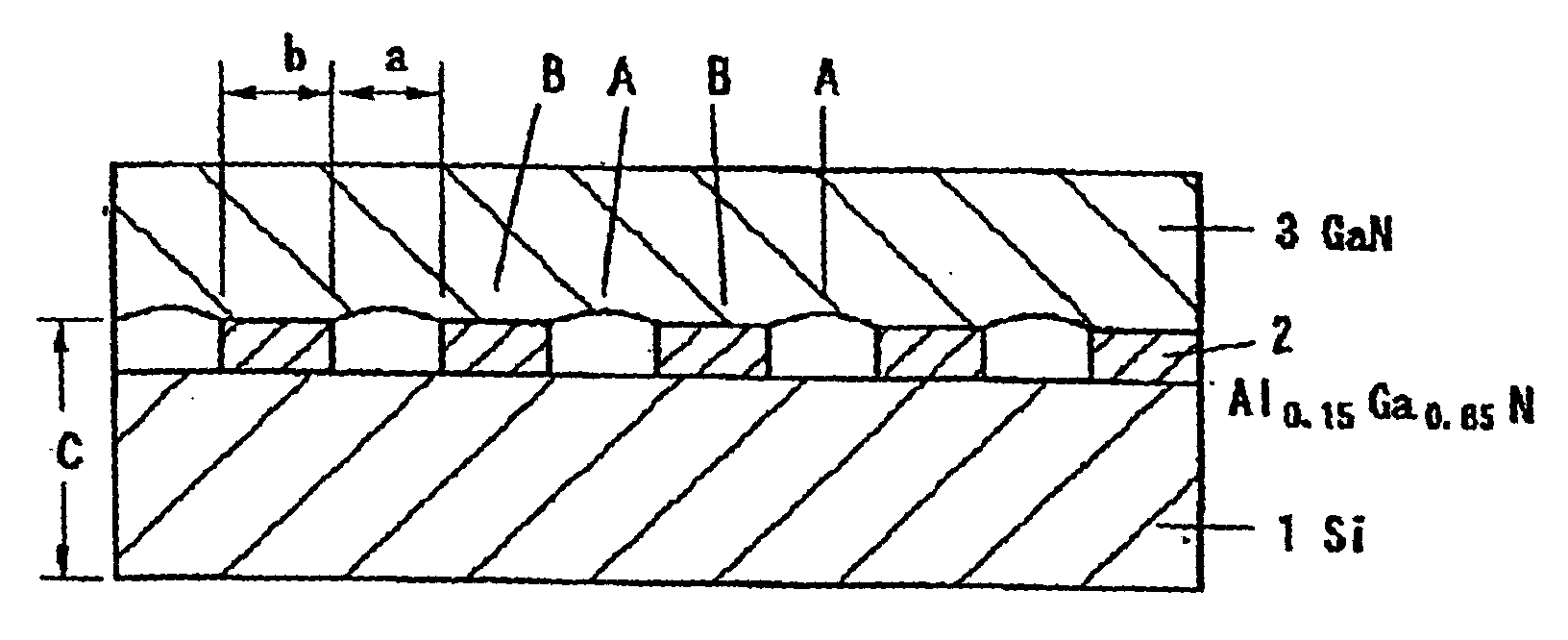
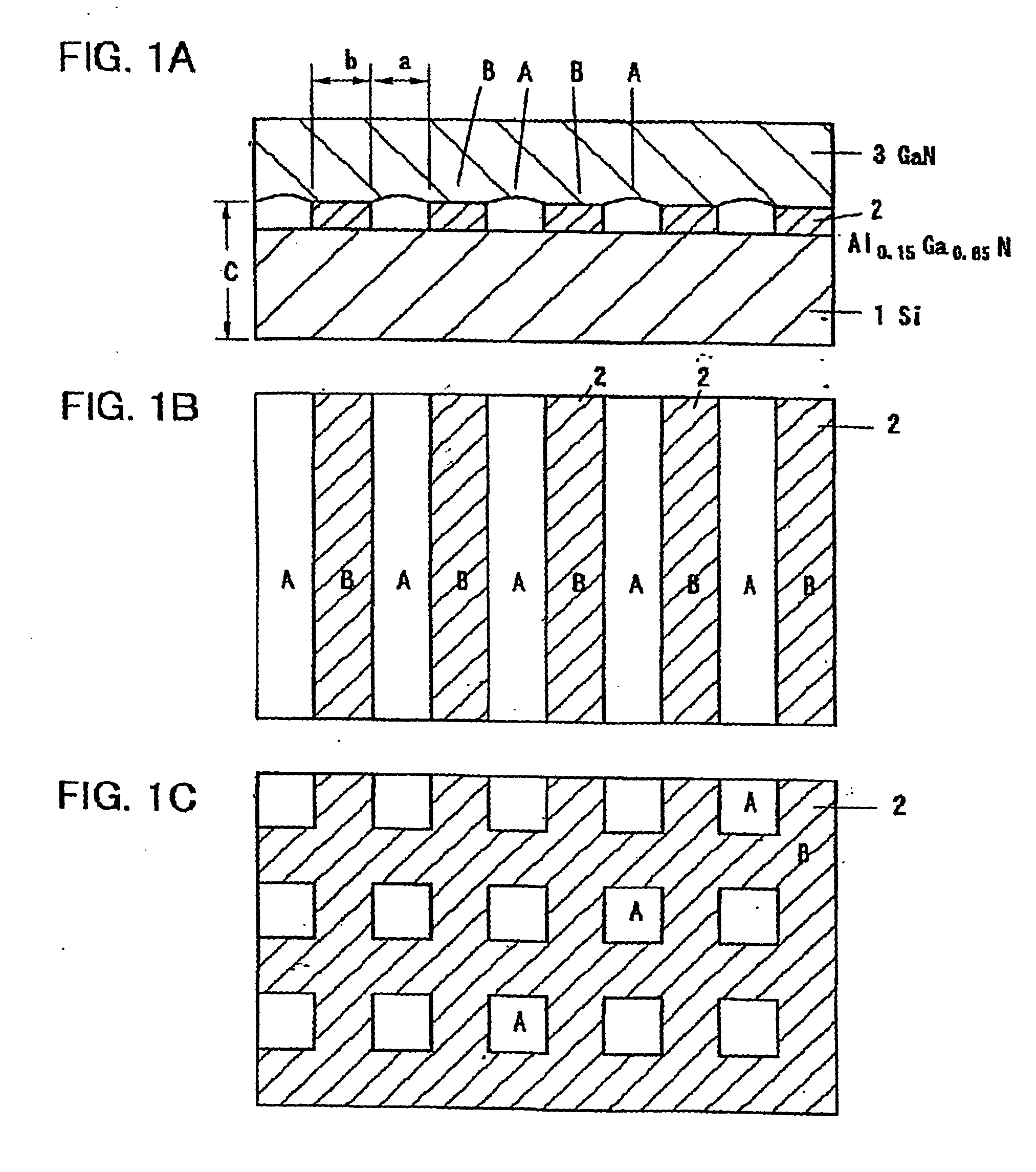
[0017]FIG. 1 is a schematic sectional view showing the structure of a gallium nitride group compound semiconductor according to a first embodiment of the present invention. On a silicon substrate 1, an Al0.15Ga0.85N layer (layer of a first gallium nitride group compound semiconductor) 2 having a thickness of about 1000 Å is formed in a striped pattern (FIG. 1(b)) or a grid pattern (FIG. 1(c)). A GaN layer (layer of a second gallium nitride group compound semiconductor) 3 having a thickness of about 10 μm is formed in regions A where the layer 2 is removed from the substrate 1 and in regions B which are defined above the islands of the layer 2.
[0018] Next, a process for manufacturing the gallium nitride group compound semiconductor will be described.
[0019] The semiconductor is formed through the use of a sputtering method and a metal organic vapor phase epitaxy (hereinafter referred to as “MOVPE”) method. Gases used in the MOVPE method are ammonia (NH3), ca...
second embodiment
[0028] (Second Embodiment)
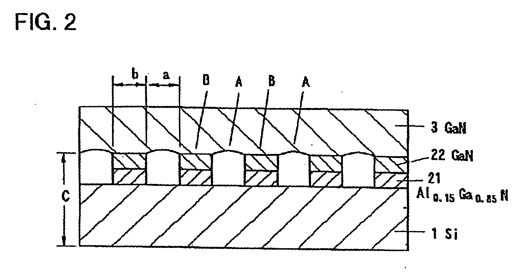
[0029] In the first embodiment, only one layer; i.e., the Al0.15Ga0.85N layer 2, is formed as a layer of the first gallium nitride group compound semiconductor. The present embodiment is characterized in that two layers; i.e., an Al0.15Ga0.85N layer 21 and a GaN layer 22, are formed, in this sequence, as the layer of the first gallium nitride group compound semiconductor.
[0030]FIG. 2 is a sectional schematic view showing the structure of a gallium nitride group compound semiconductor according to a second embodiment of the present invention. The Al0.15Ga0.85N layer 21 is formed on the silicon substrate 1 to a thickness of about 1000 Å, and the GaN layer 22 is formed on the layer 21 to a thickness of about 1000 Å. The layer 21 and the layer 22 constitute the layer of the first gallium nitride group compound semiconductor. The layer 21 and the layer 22 are formed in a striped or grid pattern as in the first embodiment. The GaN layer 3 having a thickness of a...
PUM
| Property | Measurement | Unit |
|---|---|---|
| thickness | aaaaa | aaaaa |
| flow rate | aaaaa | aaaaa |
| width | aaaaa | aaaaa |
Abstract
Description
Claims
Application Information


