Electrical interconnection, method of forming the electrical interconnection, image sensor having the electrical interconnection and method of manufacturing the image sensor

Inactive Publication Date: 2005-01-06
SAMSUNG ELECTRONICS CO LTD
View PDF6 Cites 47 Cited by
  • Summary
  • Abstract
  • Description
  • Claims
  • Application Information

AI Technical Summary

Benefits of technology

[0017] At least one of the above and other features and advantages of the present invention may be realized by providing an electrical interconnection including a first insulation layer formed on a substrate, a first metal pattern, a first diffusion barrier layer formed on the first insulation layer and the first metal pattern, a second insulation layer formed on the diffusion barrier layer, and a second metal pattern. The first insulation layer includes at least a first recessed portion, and the first metal pattern fills the first recessed portion. The first diffusion barrier layer prevents the diffusion of a metal material of the first metal pattern. The second insulation layer includes at least a second recessed portion that exposes an upper surface of the first metal pattern, and the second metal pattern fills the second recessed portion.
[0018] At least one of the above and other features and advantages of the present invention may be realized by providing a method of forming an electrical interconnection including forming a first insulating layer on a semiconductor substrate such that at least a first recessed portion is formed therein. Then, the first recessed portion is filled with metal to form a first metal pattern. A first diffusion barrier layer is then formed on the first metal pattern and the first insulation layer. The first diffusion barrier layer includes a metal oxide, and prevents the diffusion of metal out of the first metal pattern. Next, a second insulation layer is formed on the first diffusion barrier layer such that the second insulation layer includes at least a second recessed portion exposing a portion of the first metal pattern. The second recessed portion is filled with metal, thereby forming a second metal pattern.
[0019] At least one of the above and other features and advantages of the present invention may be realized by providing an image device including a substrate, an insulating interlayer structure, a plurality of metal patterns, a plurality of diffusion barrier layers including aluminum oxide, a color filter, and a lens. A semiconductor device including an optoelectronic device is disposed on the substrate. The insulating interlayer structure includes a plurality of insulating interlayer patterns stacked therein, and each of the insulating interlayer pa

Problems solved by technology

The resulting reduced feature size increases the difficulty of forming electrical interconnections on a semiconductor substrate.
The increased difficulty in forming wirings imposes strict requisites on a metal layer forming electrical interconnections on the substrate.
However, aluminum and tungsten have high specific resistances of 2.8×10⁻⁸ Ωm and 5.5×10⁻⁸ Ωm, respectively, and thus are not suitable for a multi-layer structure.
A reactive ion

Method used


Image

  • Electrical interconnection, method of forming the electrical interconnection, image sensor having the electrical interconnection and method of manufacturing the image sensor
  • Electrical interconnection, method of forming the electrical interconnection, image sensor having the electrical interconnection and method of manufacturing the image sensor
  • Electrical interconnection, method of forming the electrical interconnection, image sensor having the electrical interconnection and method of manufacturing the image sensor

Examples


Embodiment Construction

[0030] Korean Patent Application No. 2003-44099, filed on Jul. 1, 2003, in the Korean Intellectual Property Office, and entitled: “Metal Wiring, Method of forming the Metal Wiring, Image Sensor Having the Metal Wiring and Method of Manufacturing the Image Sensor,” is incorporated by reference herein in its entirety.

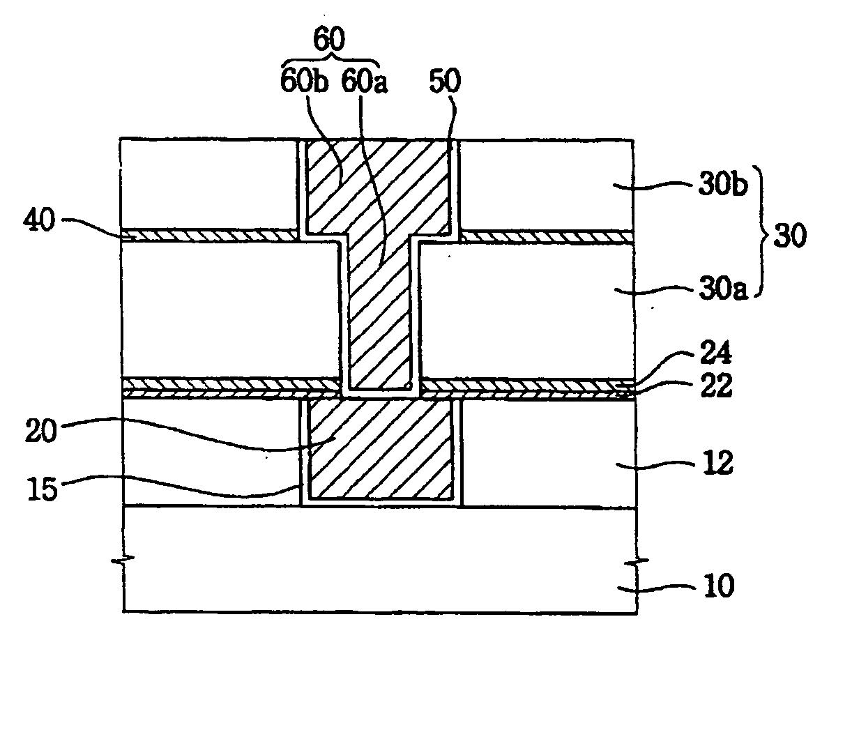
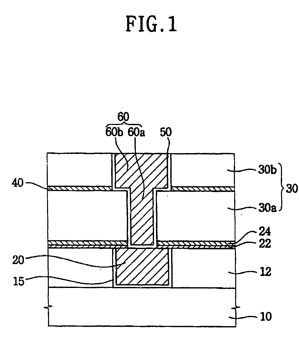
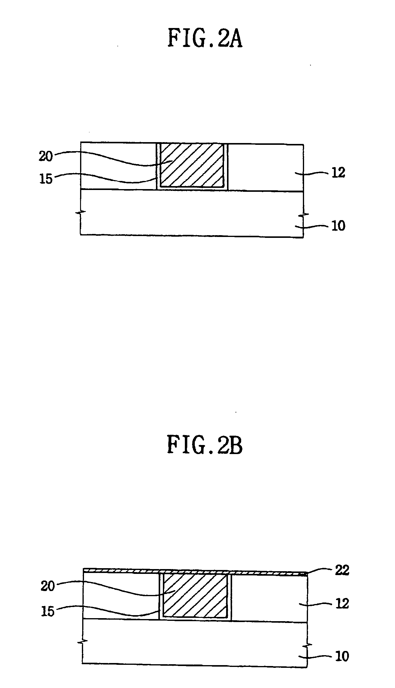
[0031] The present invention now will be described more fully hereinafter with reference to the accompanying drawings, in which embodiments of the invention are shown. This invention may, however, be embodied in many different forms and should not be construed as limited to the embodiments set forth herein; rather, these embodiments are provided so that this disclosure will be thorough and complete, and will fully convey the scope of the invention to those skilled in the art. In the drawings, the thickness of layers and regions are exaggerated for clarity. Like reference numerals refer to similar or identical elements throughout. It will be understood that when an elemen...


PUM


Abstract

An electrical interconnection for a highly integrated semiconductor device includes a first insulation layer having at least a first recessed portion on a substrate. The first recessed portion is filled with metal to form a first metal pattern. A diffusion barrier layer including aluminum oxide of high light transmittance is provided on the first insulation layer and the first metal pattern for preventing metal from diffusing. An insulating interlayer including a second recessed portion for exposing an upper surface of the first metal pattern is provided on the diffusion barrier layer. The second recessed portion is filled with metal to form a second metal pattern. The electrical interconnection may be used with an image sensor. The metal may be copper. High light transmittance of the diffusion barrier layer ensures external light reaches the photodetector. The aluminum oxide of the diffusion barrier layer reduces parasitic capacitance of the electrical interconnections.

Description

BACKGROUND OF THE INVENTION [0001] 1. Field of the Invention [0002] The present invention relates to an electrical interconnection and a method of forming the electrical interconnection, and to an image sensor having the electrical interconnection and a method of manufacturing the image sensor. More particularly, the present invention relates to an electrical interconnection of copper and a method of forming the electrical interconnection, and to a complementary metal oxide semiconductor (CMOS) image sensor having the electrical interconnection of copper and a method of manufacturing the CMOS image sensor. [0003] 2. Description of the Related Art [0004] The availability and use of information media and equipment for processing information media, e.g., computers, has been steadily increasing. Components using semiconductor technology are under pressure to keep pace with these developments. These developments require semiconductor devices that operate at a high speed and having a larg...

Claims


Application Information

Patent Timeline
IPC IPC(8): H01L23/532H01L21/3205H01L27/146
CPCH01L23/53238H01L23/53295H01L27/14683H01L27/14636H01L27/14601H01L2924/0002H01L2924/00H01L21/3205
Inventor WON, SEOK-JUN
Owner SAMSUNG ELECTRONICS CO LTD
Why Eureka
Try Eureka