
Substrate noise analyzing method for semiconductor integrated circuit, semiconductor integrated circuit, and substrate noise analyzing device for semiconductor integrated circuit

a technology of semiconductor integrated circuits and substrate noise, which is applied in the direction of error detection/correction, program control, instruments, etc., can solve the problems of substrate noise, large degraded performance of analog circuits, and large increase in the magnitude of substrate nois

Inactive Publication Date: 2005-01-06
PANASONIC CORP
View PDF4 Cites 16 Cited by
  • Summary
  • Abstract
  • Description
  • Claims
  • Application Information

AI Technical Summary

Benefits of technology

[0025] It is an object of the invention to provide a substrate noise analyzing method that allows substrate noise caused by combinations of fluctuations in power supply current, ground current, power supplies, grounds and circuit elements to be analyzed at high speed.

Problems solved by technology

The circuit elements are electrically connected with one another through the semiconductor substrate, so that potential fluctuations at the substrate generated by the operation of a circuit element are propagated to other circuit elements, and affect them as substrate noise.
In recent years, an enormous number of circuits are integrated, and the magnitude of the substrate noise has increased accordingly.
In a system LSI having various functions provided in a single semiconductor integrated circuit in particular, both digital and analog circuits are provided on the same semiconductor substrate, and therefore the performance of the analog circuits is greatly degraded by the substrate noise.
The noise that could affect audio and video qualities is recognized after the semiconductor integrated circuit is completed, which has come to be a serious problem.
The current is transmitted to the substrate of the transistors ANchTr and APchTr in the analog circuit through the substrate contacts DPsubcon and DNsubcon or the sources of the transistors DNchTr and DPchTr and thus makes the operation unstable.
This vibration is transmitted to the substrate of the transistors ANchTr and APchTr in the analog circuit and makes the operation of the transistors unstable.
As a result, clock signals generated by a PLL that is often used for an analog configuration can be unstable or the conversion precision of the analog-digital (A / D) conversion circuit can be degraded.
This is a serious problem particularly in a high density, large scale system LSI whose power supply current and power supply fluctuations are great.
The method however employs a method of summing only ground current and contact resistance on a mesh basis related to the substrate structure, and substrate noise caused by combinations of fluctuations of circuit elements and power supplies cannot be expressed well.

Method used


Image

  • Substrate noise analyzing method for semiconductor integrated circuit, semiconductor integrated circuit, and substrate noise analyzing device for semiconductor integrated circuit
  • Substrate noise analyzing method for semiconductor integrated circuit, semiconductor integrated circuit, and substrate noise analyzing device for semiconductor integrated circuit
  • Substrate noise analyzing method for semiconductor integrated circuit, semiconductor integrated circuit, and substrate noise analyzing device for semiconductor integrated circuit

Examples


fourth embodiment

[0041] the invention is related to a method of calculating current passed through a substrate from circuit elements at high speed.

[0042] Fifth to eighth embodiments of the invention are related to a method of summing information based on simultaneous fluctuations, blocks, names, and regions.

[0043] Ninth to twelfth embodiments of the invention are related to a method of summing circuit element current, power supply-ground current, junction capacitance, interface resistance, and power supply-ground resistance in the above described summing ranges.

first embodiment

[0044] (First Embodiment)

[0045] The first embodiment of the invention will be described. According to the embodiment, current forms at the ground or power supply are estimated based on fluctuations in the logical values in digital simulation or functional simulation in order to increase the speed of analyzing substrate noise.

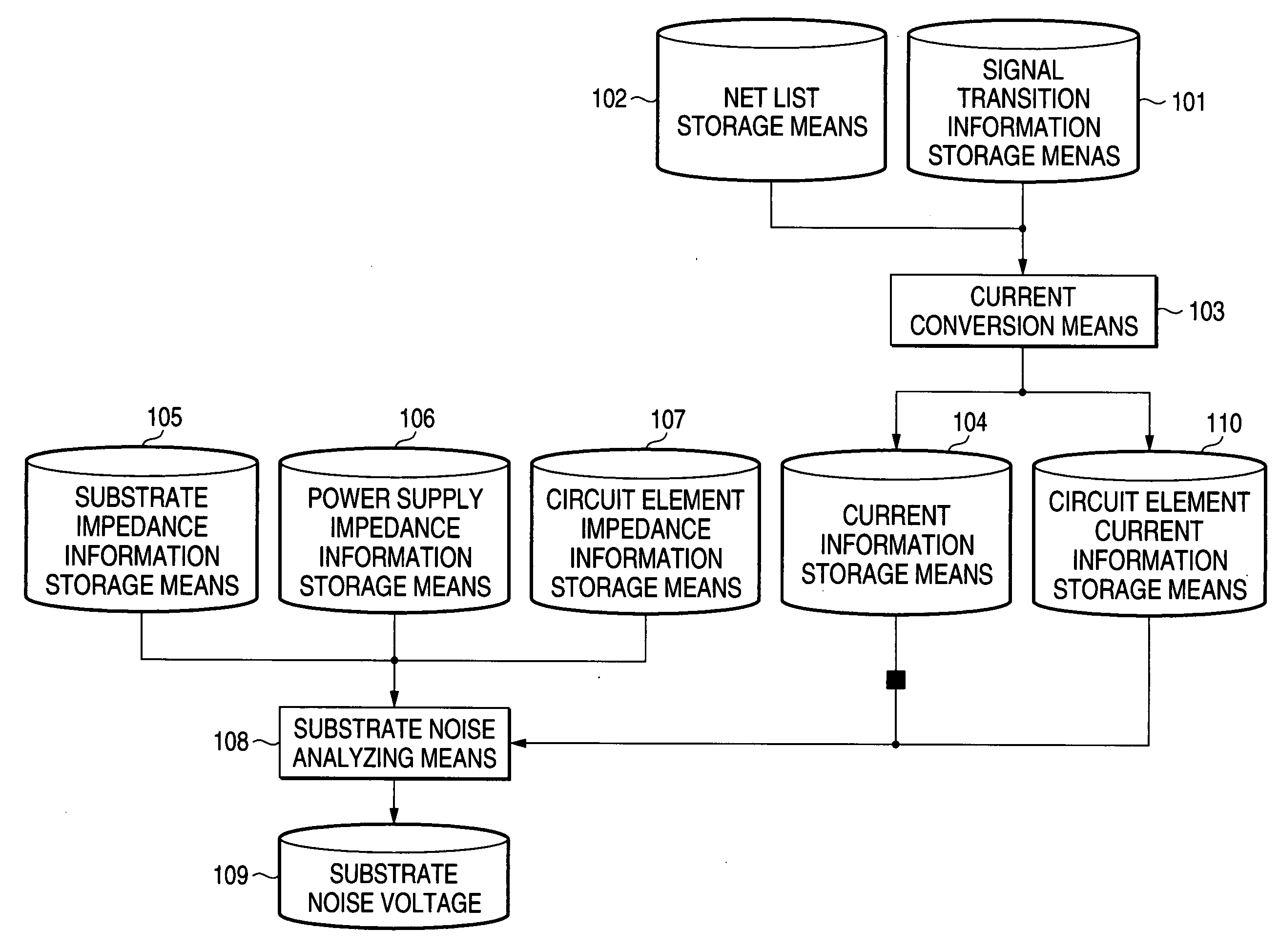
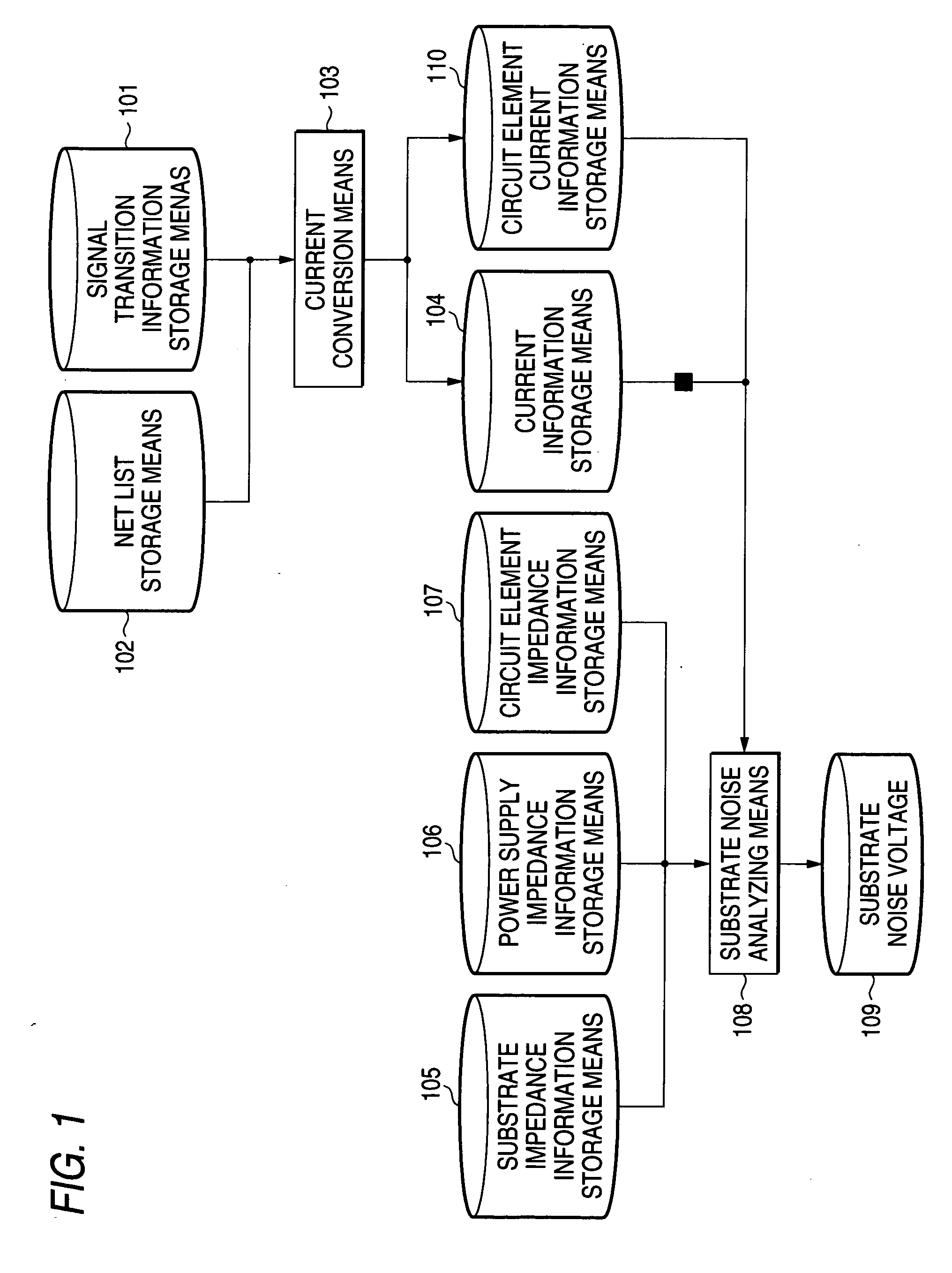
[0046]FIG. 1 shows the first embodiment.

[0047] Current conversion means 103 reads line capacitance made of the parasitic capacitance information of output lines of the circuit elements and / or information on the next stage circuit elements from net list storage means 102 that stores the net list of a semiconductor integrated circuit to be analyzed. Then, the current conversion means 103 converts the line capacitance into current fluctuations on the power supply side and ground side based on signal transitions between the logical states 0 and 1 at the output terminals of the circuit elements read from signal transition information storage means 101 that stores t...

second embodiment

[0054] (Second Embodiment)

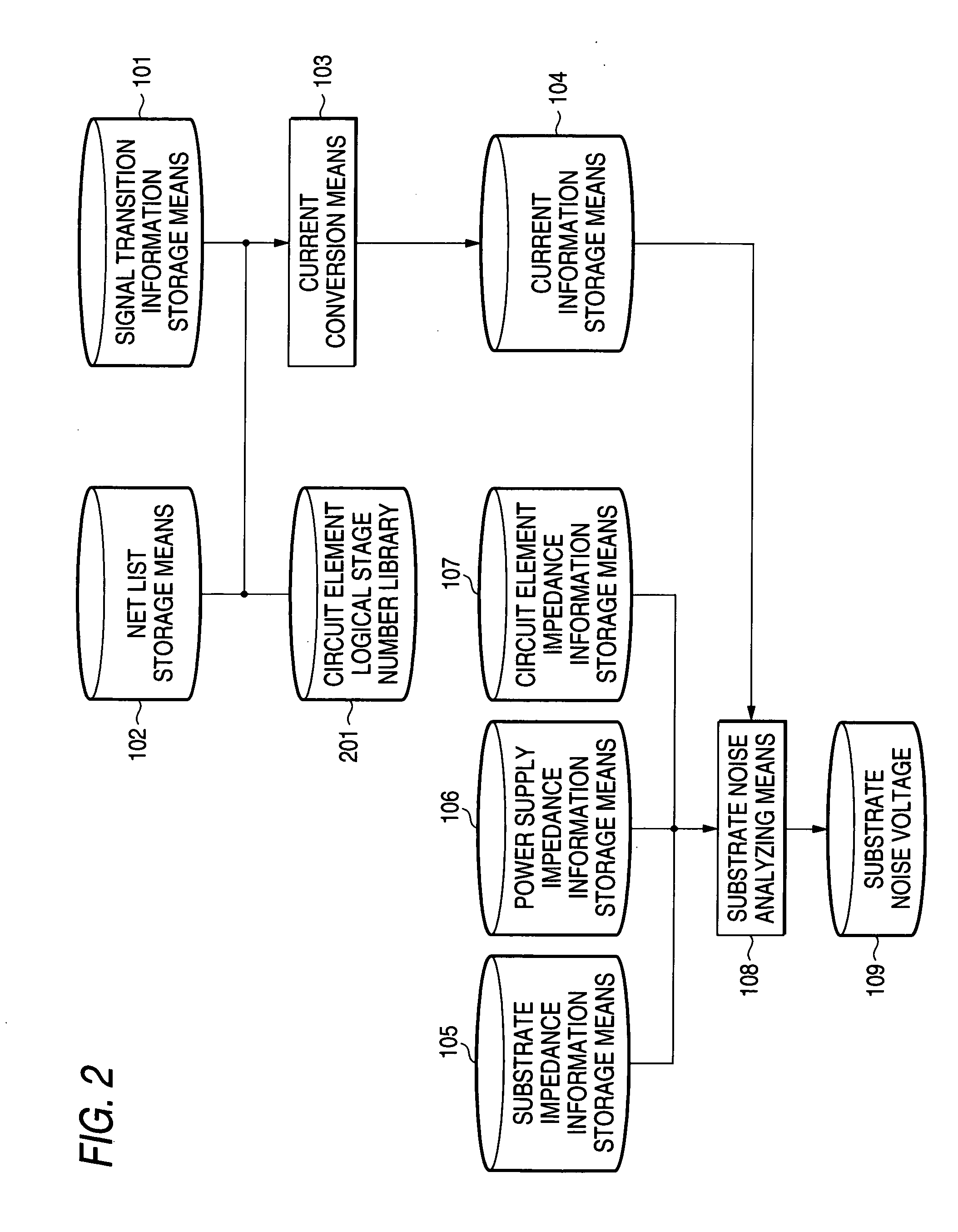
[0055] The second embodiment of the invention will be described. In place of the first embodiment, the second embodiment is directed to a method of estimating the current waveform at the ground and the power supply based on library information having the number of logical stages in a cell.

[0056] The number of logical stages is defined as the number of channel-connect structures (CCC). For example, three stages of inverters as shown in FIG. 19 can be separated into 1901, 1902, and 1903 as structures connected through channels (separated by gates) In this case, the number of logical stages is three. The number of logical stages is previously formed into a library on a logical element basis as shown in FIG. 20, and stored in the circuit element logical stage number library storing means 201. When current is calculated by the current conversion means 103 using the logical stage number information, current fluctuations generated in a internal logical element is...


PUM


Abstract

In substrate noise analysis for a semiconductor integrated circuit, it takes long to calculate the amount of current input to the substrate and substrate potential fluctuations in an analog circuit to which the current is propagated in combination with impedance / power supply resistance of the substrate including a large scale RC circuit network. The amount of calculation is reduced in calculating current passed to power supply / ground by adding triangles having areas corresponding to power consumption separately for rising / falling in logical changes in gate level simulation. The amount of calculation is reduced by summing current, interface capacitance, interface resistance, power supply resistance, ground resistance, power supply voltage fluctuations, and ground voltage fluctuations on a basis of block, instance or simultaneous operation. Since the calculation amount is reduced, it takes a shorter period to apply substrate noise analysis. In addition, the elements for calculation are also reduced, and therefore substrate noise analysis can be applied to a large scale semiconductor integrated circuit.

Description

[0001] The present application is based on Japanese Patent Application No. 2003-163626, which is incorporated herein by reference. BACKGROUND OF THE INVENTION [0002] 1. Field of the Invention [0003] The present invention relates to an analyzing technique for a semiconductor integrated circuit, and more particularly to a substrate noise analyzing method by simulation related to noise through substrate impedance in a semiconductor integrated circuit and a substrate noise analyzing device that carries out the method. The invention also relates to a semiconductor integrated circuit device subjected to the process by the substrate noise analyzing method [0004] 2. Description of the Related Art [0005] In forming a semiconductor integrated circuit, impurity is diffused on a semiconductor substrate to form elements, while layers of metal are placed to form interconnections, and in this way, circuits are integrated. The circuit elements are electrically connected with one another through the...

Claims


Application Information

Patent Timeline
IPC IPC(8): G06F9/45G06F17/50H01L21/82
CPCG06F17/5036G06F30/367
Inventor HIRANO, SHOUZOUSHIMAZAKI, KENJITSUJIKAWA, HIROYUKI
Owner PANASONIC CORP
Learn More