Organic semiconductor devices and methods of fabrication

a technology of organic materials and semiconductor devices, applied in the direction of sustainable manufacturing/processing, final product manufacturing, nanoinformatics, etc., can solve the problems of inflexible sequential methods, compatibility of materials, and the choice of solvents still remains a problem, so as to achieve flexibility and versatility.

Active Publication Date: 2005-01-13
MERCK PATENT GMBH
View PDF2 Cites 58 Cited by
  • Summary
  • Abstract
  • Description
  • Claims
  • Application Information

AI Technical Summary

Benefits of technology

[0006] One objective of this invention is to provide an organic materials-based semiconductor device with two parts, a first part is formed on a first substrate with a first electrode and at least one first organic layer and a second part is formed on a second substrate with a second electrode and at least one second organic layer. These two parts are combined to form the final device. This combinatorial process provides versatility and flexibility in constructing organic materials-based semiconductor device. Another objective is to provide methods for fabrication of the organic materials-based semiconductor devices with two parts, particularly, methods of assembling the two parts into a single device.

Problems solved by technology

One major drawback of this sequential fabrication is the requirements to integrate the wet processes and the dry processes, with total different working environments, into a single fabrication chamber.
Even though various layers on top of each other can be processed by wet processing method, the choice of solvent still remains a problem, because the solvent used for one layer may attack the previously coated layer.
Another drawback of the sequential fabrication of the successive layers to form the organic devices is the compatibility of the materials, specifically the ones for anode and cathode.
This sequential method is not flexible enough to meet the requirements for a roll-to-roll process, especially for the production of larger size flat devices.

Method used


Image

  • Organic semiconductor devices and methods of fabrication
  • Organic semiconductor devices and methods of fabrication
  • Organic semiconductor devices and methods of fabrication

Examples


example 1

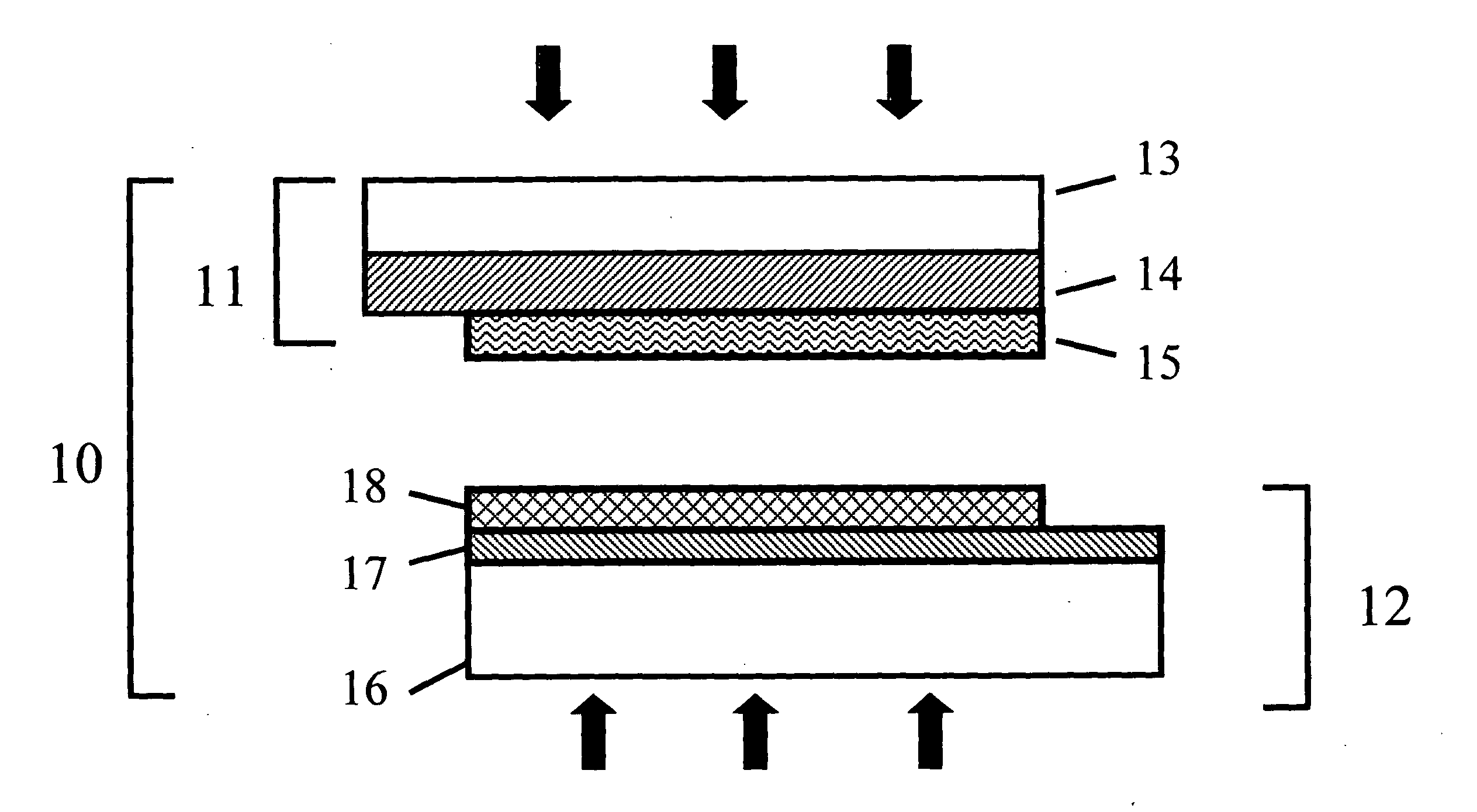
The Formation of the First Part (11) with a Light-Emitting Polymer

[0026] A layer of nickel was first deposited onto a glass substrate by conventional coating methods. Then onto the top surface of nickel, a layer of semiconducting polymer MEH-PPV (structure shown in FIG. 6(a)) is spin-coated from a 1% wt. / v of MEH-PPV in toluene at 2000 rpm. A low temperature heat treatment of the sample with the semiconducting polymer is now carried out to vaporize the solvent trapped within the polymer and to improve the molecule arrangement within the film. The heat treatment may be carried out in an inert atmosphere at a temperature in a range of 80° C. to 120° C., for a period ranging from 30 minutes to about 120 minutes, depending on the type of polymer used. This completes the construction of the first part (11) of an organic semiconductor device (10) that consists a nickel cathode covered by a semiconductor polymer, i.e, Glass / Ni / MEH-PPV, where the glass is the first substrate (13), nickel c...

example 2

The Construction of the Second Part (12) with a Hole Transport Layer

[0027] In a chamber with flowing inert gas such as nitrogen, argon or a mixture of them, a commercial ITO-coated glass is pre-cleaned by a conventional technique. A layer of PEDOT is then spin-coated onto the ITO-coated glass from a commercially available PEDOT solution. This PEDOT-coated ITO glass will serve as the second part (12) of the organic semiconductor device (10), where the glass is the second substrate (16), ITO is the second electrode (17) and PEDOT makes up the second organic material layer (18) according to FIG. 3.

example 3

The Construction of an OLED

[0028] Example 1 provides the construction of the first part (11) of an organic semiconductor device (10). It consists of the first glass substrate (13), the first electrode (14) and the first organic semiconductor material (15), with a structure of Glass / Ni / MEH-PPV. Example 2 provides the second part (12) of an organic semiconductor device (10) and it has a structure of Glass / ITO / PEDOT, where the glass is the second substrate, ITO is the second electrode (17) and the PEDOT is the second organic semiconductor material (18). An OLED device (10) is then fabricated by stacking the first part (11) with the second part (12), and this delivers a final device structure of Glass / ITO / PEDOT / MEH-PPV / Ni / Glass. To have a better interface contact between the first part (11) and the second part (12), the two parts may be pressed while being heated. A conventional encapsulation with epoxy resin is finally carried out before the further characterization of this OLED.


PUM

PropertyMeasurementUnit
temperatureaaaaaaaaaa
thicknessaaaaaaaaaa

Abstract

This invention discloses structures of organic materials-based semiconductor devices and methods for the fabrication of such devices. According to this invention, each of the devices has a first part and a second part. The first part has at least a first organic semiconductor material layer deposited on a first electrode and the second part has at least a second organic semiconductor material layer deposited on a second electrode. Said device is formed by assembling the two individual parts together. Each part maybe fabricated separately and consists of an electrode coated with semiconductor organic materials required by the function of the desired device. A schematic diagram in the FIG. 3 shows a first part (11) consisting of a first substrate (13), a first electrode (14) and at least one layer of organic materials (15); the second part (12) of the device consisting of the second substrate (16), a second electrode (17) with at least a layer of organic materials (18). The organic device (10) is finally obtained by combining the first part (11) with the second part (12) under controlled environment. This is preferably done by aligning the first part (11) onto the second part (12), and then by initiating a cross-link between organic material (15) and organic material (18) via heating, electron beam or light irradiation.

Description

FIELD OF THE INVENTION [0001] This invention relates to structures of organic materials-based semiconductor devices and the methods of fabrication the same. BACKGROUND OF THE INVENTION [0002] From light emitting diodes, solar cells, sensors, transistors to many other semiconductor devices, organic materials with controllable electronic and opto-electronic properties are emerging as potential competitors to silicon, gallium aresenide and other inorganic semiconductor materials as the backbones of the semiconductor industry [J. M. Shaw, P. F. Seidler, IBM Journal of Research &Development, 45(1), 3(2001)]. [0003] A simple organic semiconductor device may consist of one layer of electro-opto active organic materials sandwiched between two electrodes. However in practice, many layers of organic semiconductor materials with different energy levels and functionalities are often required in order to improve the device performance. One typical example is an organic light-emitting device (OLE...

Claims


Application Information

Patent Timeline
Patent Type & Authority Applications(United States)
IPC IPC(8): H01L21/00H01L35/24H01L51/00H01L51/30H01L51/40H01L51/56
CPCB82Y10/00H01L51/0024H01L51/0036H01L51/0037H01L51/0038H01L51/0039Y02E10/549H01L51/0046H01L51/424H01L51/4253H01L51/56H01L2251/308H01L51/0043Y02P70/50H10K71/50H10K85/114H10K85/115H10K85/113H10K85/211H10K85/151H10K85/1135H10K30/20H10K30/30H10K2102/103H10K71/00
Inventor XIAO, STEVEN SHUYONGQIU, CHUNONGQIU, CINDY XING
Owner MERCK PATENT GMBH
Why Eureka
Try Eureka