Novel method to achieve increased trench depth, independent of CD as defined by lithography

Inactive Publication Date: 2005-01-13
IBM CORP
View PDF10 Cites 20 Cited by
  • Summary
  • Abstract
  • Description
  • Claims
  • Application Information

AI Technical Summary

Benefits of technology

[0022] forming an epitaxial silicon film on at least some portions of said sidewalls s

Problems solved by technology

Thus, with less charge to detect, reading the information or data from the memory cell becomes much more difficult.
For example, solution (1), which thins the capacitor dielectric, also increases leakage currents that may affect the memory retention performance of the capacitor and the reliability of the memory cell.
Moreover, the substitution of alternative dielectrics may be more complicated, more expensive and provide fabrication problems that are heretofore unknown.
However, the depth of the trench is

Method used


Image

  • Novel method to achieve increased trench depth, independent of CD as defined by lithography
  • Novel method to achieve increased trench depth, independent of CD as defined by lithography
  • Novel method to achieve increased trench depth, independent of CD as defined by lithography

Examples


first embodiment

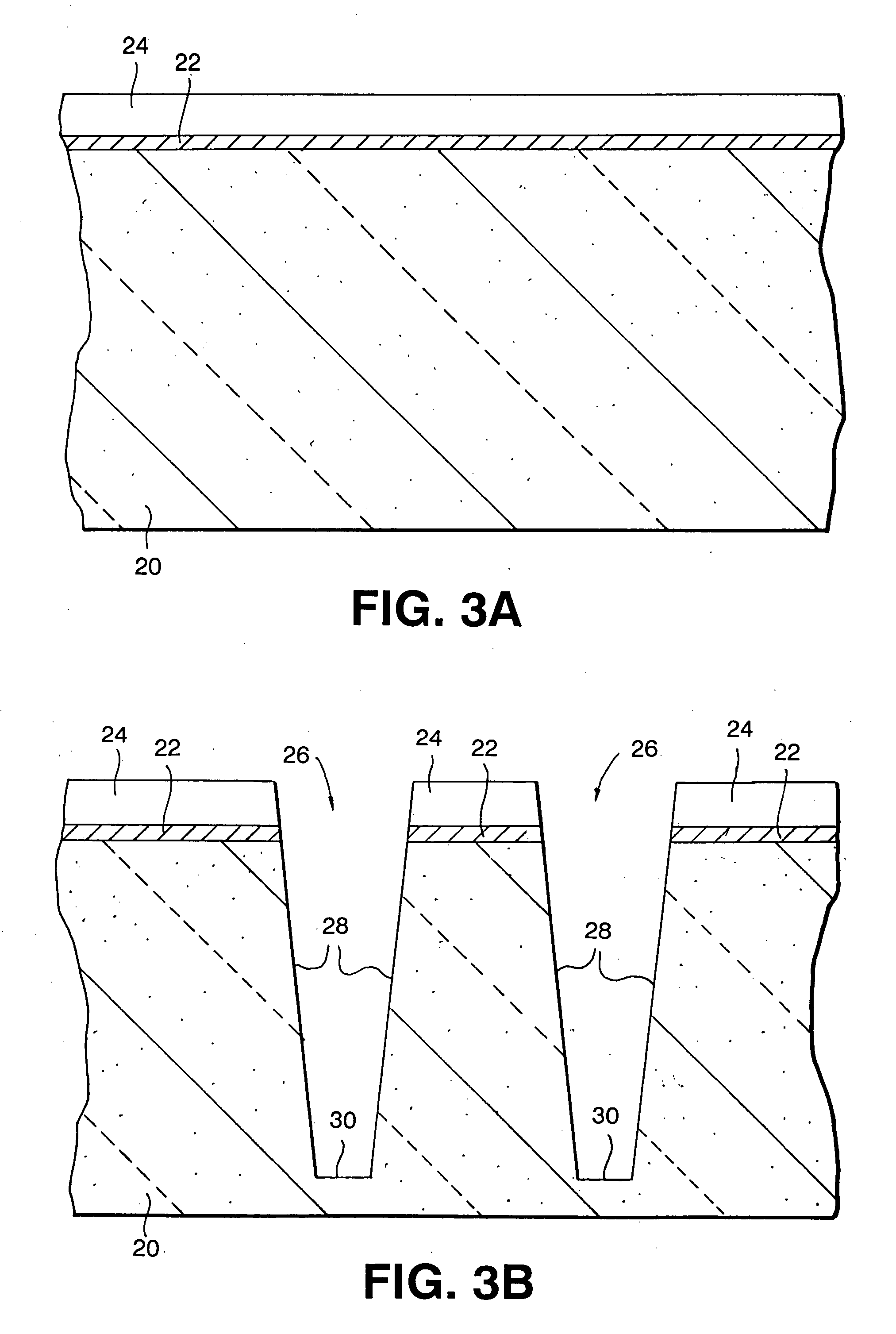
[0034] The above basic processing steps will be further described in conjunction with the following three embodiments. Reference is first made to FIGS. 3A-3E which illustrate the present invention. Specifically, FIG. 3A shows an initial structure that is employed in the present invention. The initial structure shown in FIG. 3A comprises substrate 20, pad layer 22 present atop a surface of substrate 20 and mask 24 present atop pad layer 22. The structure shown in FIG. 3A is fabricated using conventional processing steps that are well known to those skilled in the art and the illustrated structure includes conventional materials that are also well known to those skilled in the art.

[0035] For example, substrate 20 comprises any semiconducting material including, but not limited to: Si, Ge, SiGe, GaAs, InAs, InP and all other III / V semiconductor compounds. Layered substrates containing the same or different semiconducting material such as Si / SiGe, and silicon-on-insulators (SOIs) are al...

third embodiment

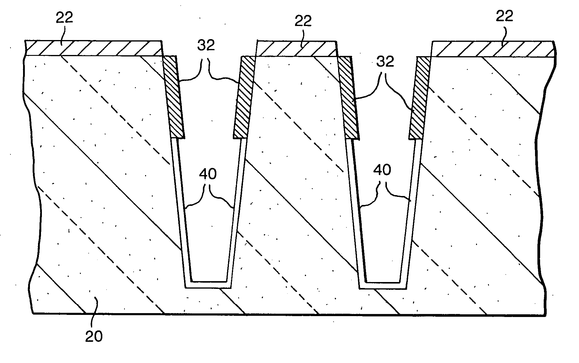
[0054] In accordance with the present invention, selective epitaxial silicon film 32 is formed only on upper sidewalls of each deep trench where device connections, such as buried straps, are later fabricated, leaving the bottom portion of the trench untouched. To achieve formation of the epitaxial silicon film on the upper sidewalls of each deep trench, liner 40 is formed on the exposed surfaces of substrate 20 within each deep trench structure using a conventional thermal growing process, a conventional deposition process or a combination thereof. Liner 40 may be composed of an oxide (formed by thermal oxidation) or an oxide / nitride stack (formed by thermal oxidation and deposition of a nitride layer). The structure including liner 40 is shown in FIG. 5A.

[0055] Each deep trench containing liner 40 is then filled with resist material 42 using a conventional deposition process and thereafter a recessed etching process is employed to remove portions of resist material 42 from the upp...


PUM


Abstract

A method of forming at least one deep trench structure having an increased trench depth is provided. The method includes providing at least one deep trench having sidewalls that extend to a common bottom wall in a surface of a substrate. Each deep trench has initial dimensions that are wider than targeted dimensions for the deep trenches. To reduce the initial dimensions to that of the targeted dimensions, an epitaxial silicon film is formed selectively or non-selectively on at least some portions of the sidewalls using a low-temperature ultra-high vacuum epitaxial silicon growth tehnique.

Description

FIELD OF THE INVENTION [0001] The present invention relates to semiconductor device manufacturing, and more particularly to a method of increasing the depth of a trench formed in a substrate which is independent of the critical deep trench mask dimensions as defined by lithography. BACKGROUND OF THE INVENTION [0002] A memory cell in an integrated circuit (IC) includes a transistor and an associated capacitor. The capacitor, which is typically formed in a portion of a trench, consists of a pair of conductive plates, i.e., electrodes, which are separated from each other by a node dielectric material. Information or data is stored in the memory cell in the form of charge accumulated on the capacitor. As the density of the ICs with memory cells is increased, the area for the capacitor becomes smaller and the amount of charge the capacitor is able to accumulate is reduced. Thus, with less charge to detect, reading the information or data from the memory cell becomes much more difficult. ...

Claims


Application Information

Patent Timeline
IPC IPC(8): H01L21/308H01L21/762H01L21/768H01L21/8242
CPCH01L21/3081H01L27/1087H01L21/76895H01L21/76224H10B12/0387
Inventor CHAN, KEVIN K.KULKARNI, SUBHASH B.MATHAD, GANGADHARA S.RANADE, RAJIV M.
Owner IBM CORP
Why Eureka
Try Eureka