Semiconductor device and method for producing it

a semiconductor and transistor technology, applied in the direction of semiconductor devices, basic electric elements, electrical appliances, etc., can solve the problems of difficult to control the influence of heat on the layers to be formed in different steps, unfavorable diffusion of gate electrode materials, and aluminum electrode materials that are problematic in that they will diffuse, etc., to achieve the effect of retarding the formation of hillocks

Inactive Publication Date: 2005-01-20
SEMICON ENERGY LAB CO LTD
View PDF99 Cites 19 Cited by
  • Summary
  • Abstract
  • Description
  • Claims
  • Application Information

AI Technical Summary

Benefits of technology

[0038] In the process, in addition, the heating induces the crystallization of the aluminum film due to the action of the titan

Problems solved by technology

This is because, in the process for producing bottom-gate-type TFT, the heating shall follow the formation of the gate electrode, by which the gate electrode material will diffuse unfavorably.
However, the electrode material of aluminum is problematic in that it will d

Method used


Image

  • Semiconductor device and method for producing it
  • Semiconductor device and method for producing it
  • Semiconductor device and method for producing it

Examples


example 1

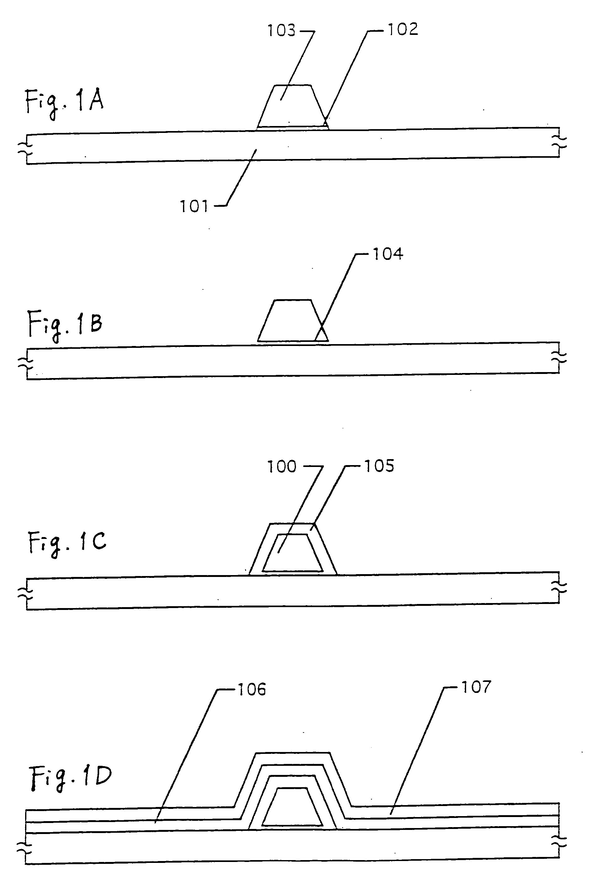
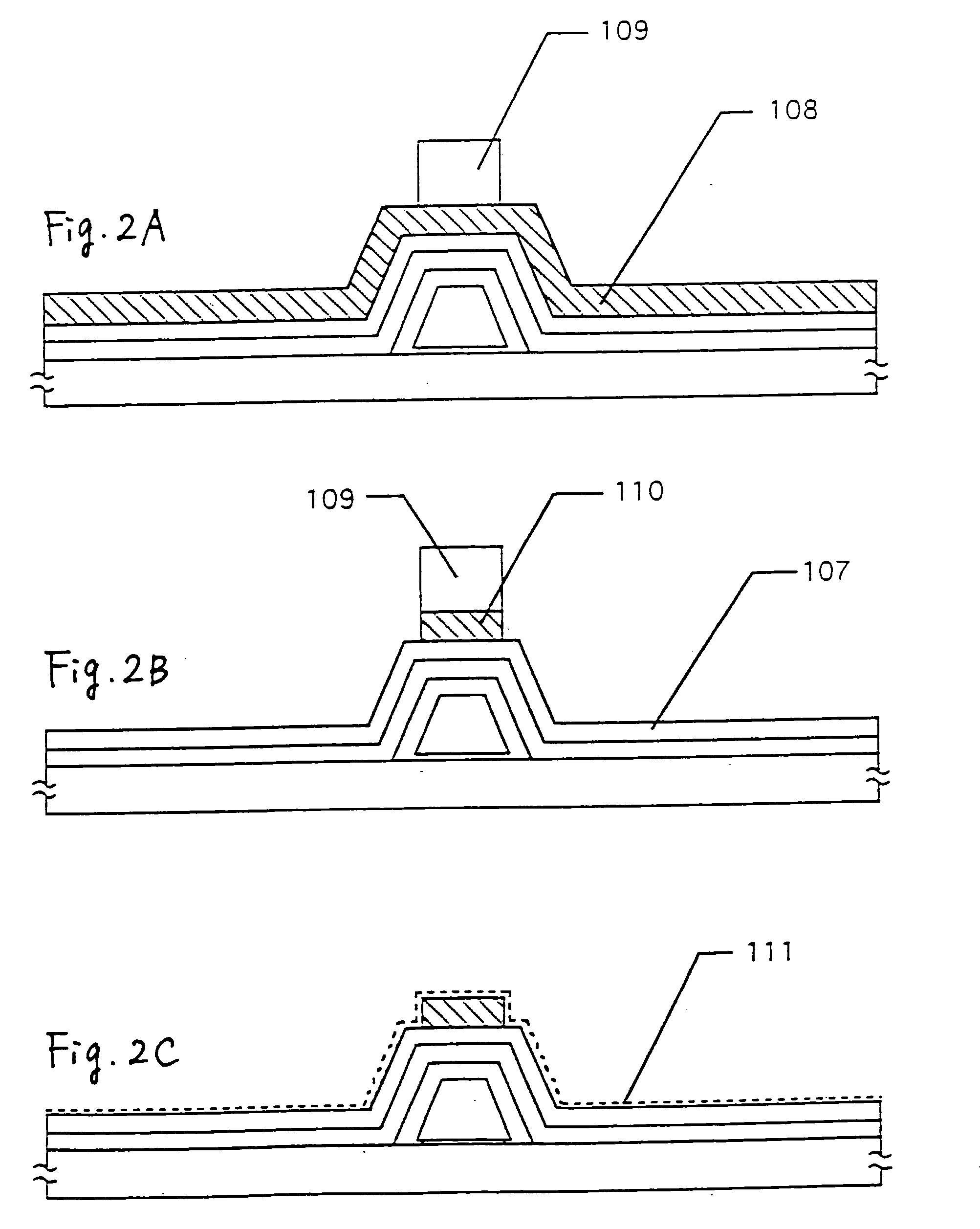
[0093]FIG. 1(A) to FIG. 1(D), FIG. 2(A) to FIG. 2(C), and FIG. 3(A) to FIG. 3(D) are referred to, which show the process of this example. First formed is a gate electrode on the glass substrate 101.

[0094] As the substrate, also usable is a quartz substrate, or a semiconductor or metal substrate having an insulating film formed thereon. The substrate of that group will be generically referred to as a substrate having an insulating surface.

[0095] In this, first, a titanium film is formed on a glass substrate through sputtering to have a thickness of 20 nm, and then an aluminum film containing 0.2% by weight of titanium is formed on the titanium film also through sputtering to have a thickness of 400 nm.

[0096] Next, the laminate film of the titanium film and the aluminum film is patterned to obtain the laminate pattern as in FIG. 1(A). The laminate pattern is composed of the titanium film pattern 102 and the aluminum film pattern 103.

[0097] To obtain this pattern, used is dry etchi...

example 2

[0141] This is to demonstrate a modification of Example 1 in which the heat treatment in the step of FIG. 3(A) was effected in a heating furnace. In this example, a heating means of so-called RTA, exposure to strong radiations, is employed for the heat treatment.

[0142] In RTA, infrared rays having been radiated by a lamp are focused on a mirror, and applied to the layered substrate, whereby the region having exposed to the focused rays is heated at a temperature falling between 600° C. and 800° C. within a short period of time.

[0143] This heat treatment utilizes the phenomenon that the region exposed to light absorbs the light. In this, therefore, the exposed region can be heated within a short period of time, and the heat treatment of the region can be finished within such a short period of time. Concretely, the heat treatment for about 1 to 10 minutes or so produces the crystallization, as in FIG. 3(A).

[0144] If desired, the heat treatment in Example 1 may be combined with RTA,...

example 3

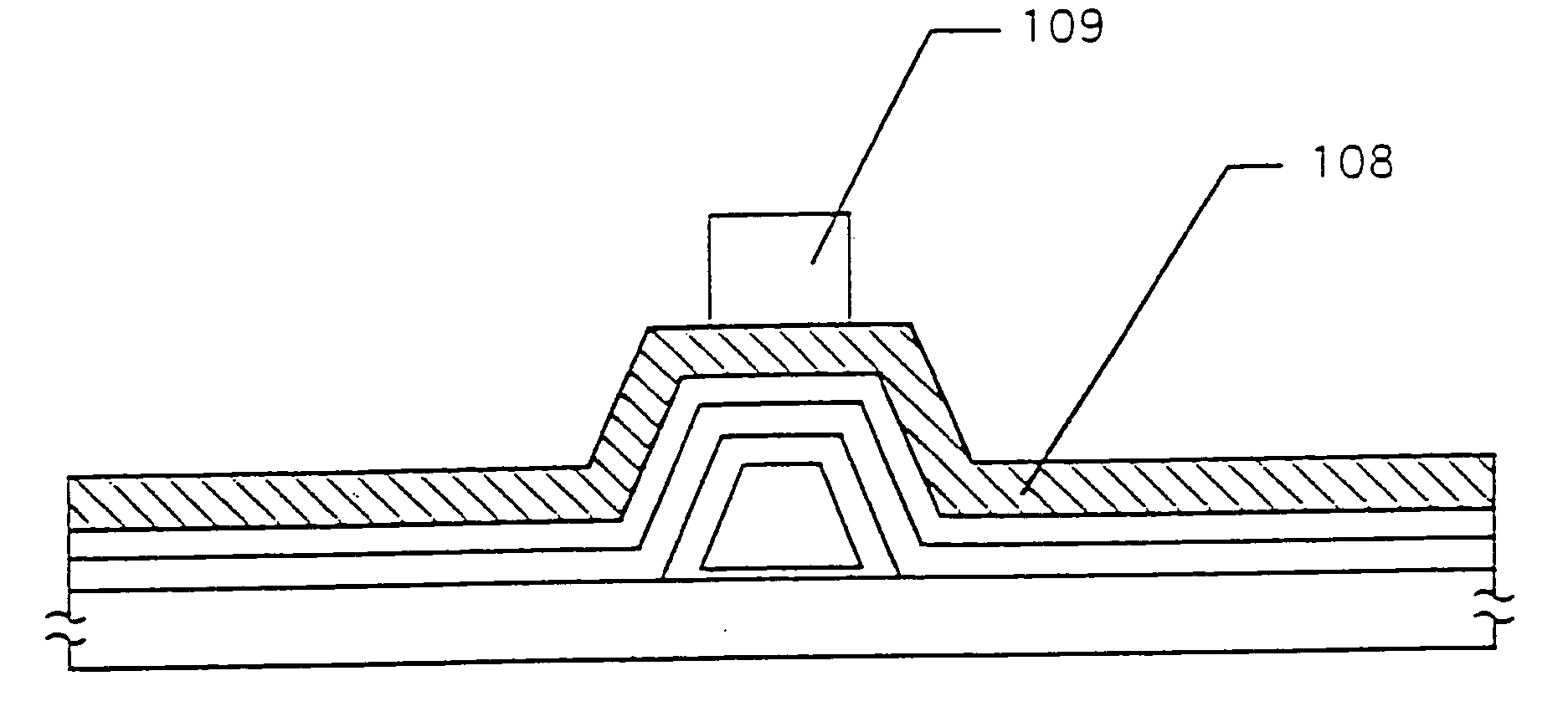
[0145] This is to demonstrate another modification of Example 1. In this example, a photo-mask is used in the step of forming the resist mask 109 in FIG. 2(A).

[0146] The process of this example has the disadvantage of requiring an increased number of masks, but has the advantage of employing conventional photolithography using a photo-mask, and the process is stable.


PUM


Abstract

Disclosed is a technique of improving the heat resistance of the aluminum gate electrode in bottom-gate-type TFT of which the active layer is made of a crystalline silicon film. A pattern of a laminate of a titanium film 102 and an aluminum film 103 is formed on a glass substrate 101. The pattern is to give a gate electrode 100. Then, the titanium film 102 is side-etched. Next, the layered substrate is heated to thereby intentionally form hillocks and whiskers-on the surface of the aluminum pattern 103. Next, the aluminum pattern 103 acting as an anode is subjected to anodic oxidation to form an oxide film 105 thereon. The anodic oxidation extends to the lower edge of the aluminum pattern 103, at which the titanium layer was side-etched. Next, a gate-insulating film 106 and an amorphous silicon film are formed. A mask is formed over the pattern, which is to give -the gate electrode, and then a nickel acetate solution is applied to the layered structure. Thus, nickel is kept in contact with the surface of the structure. Next, this is heated to induce crystal growth in the silicon film from the region contacted with nickel to the masked region. In the bottom-gate-type TFT thus produced, the active layer is made of a crystalline silicon film. In this process, since the anodic oxide film is formed as in FIG. 1(C), aluminum does neither melt to flow away nor diffuse away. Thus, the heat resistance of the aluminum electrode formed is improved.

Description

FIELD OF THE INVENTION [0001] The present invention relates to a bottom-gate-type, thin film transistor, and also to a method for producing it. BACKGROUND OF THE INVENTION [0002] Known are thin film transistors (hereinafter referred to as TFT) having an active layer of a silicon-film formed on a glass or quartz substrate. [0003] Various types of thin film transistors are known, of which, at present, bottom-gate-type ones are being most industrialized for practical use. [0004] In view of their productivity, it is desirable to develop much in future bottom-gate-type TFT to which the production process in part, the designing rule and the production equipment are common. [0005] A bottom-gate-type, thin film transistor comprises a gate electrode, a gate-insulating film and an active layer of a silicon film as formed on a substrate in that order. [0006] As the silicon film constituting the active layer, generally used is an amorphous silicon film. However, in order to obtain TFT of higher...

Claims


Application Information

Patent Timeline
IPC IPC(8): H01L21/336H01L21/77H01L21/84H01L27/12H01L29/423H01L29/49
CPCH01L27/12H01L27/14609H01L29/42384H01L27/1277H01L29/66765H01L27/124H01L29/4908H01L21/02672H01L21/3221
Inventor YAMAZAKI, SHUNPEIYAMAGUCHI, NAOAKINAKAJIMA, SETSUO
Owner SEMICON ENERGY LAB CO LTD
Why Eureka
Try Eureka